Method for producing zero layer photoetching marking of high-voltage device without barrier layers

A technology of zero-layer lithographic marking and high-voltage devices, which is applied in the field of semiconductor technology, can solve problems such as unusable, unrecognizable, and affecting the smooth process flow, so as to ensure the process flow, improve the yield rate, and ensure the smooth effect

Active Publication Date: 2013-04-10
SHANGHAI HUAHONG GRACE SEMICON MFG CORP
View PDF3 Cites 16 Cited by
  • Summary
  • Abstract
  • Description
  • Claims
  • Application Information

AI Technical Summary

Problems solved by technology

However, since the high-voltage device is directly etched and patterned on the silicon substrate, the deep trench is filled with epitaxial technology. Due to the existence of no barrier layer in the zero-layer cursor pattern, it will lead to a problem in filling the deep trench. At the same time as the trench, the epitaxial layer will also be filled in the pattern of the zero-layer lithography mark, and the deep trench filling and the silicon substrate are both single crystals. In the subsequent chemical mechanical polishing process, there is no high selectivity. If the gap is too small, the photolithographic mark cannot be recognized, which makes it impossible to use the zero-layer pattern in the subsequent process, which brings difficulties to the alignment of subsequent film layers, affects the smooth process flow, and affects the yield of the product.
[0007] like figure 1 As shown, the zero-layer lithography mark is filled by the epitaxial layer (EPI) and cannot be read

Method used


Image

  • Method for producing zero layer photoetching marking of high-voltage device without barrier layers
  • Method for producing zero layer photoetching marking of high-voltage device without barrier layers
  • Method for producing zero layer photoetching marking of high-voltage device without barrier layers

Examples


Embodiment Construction

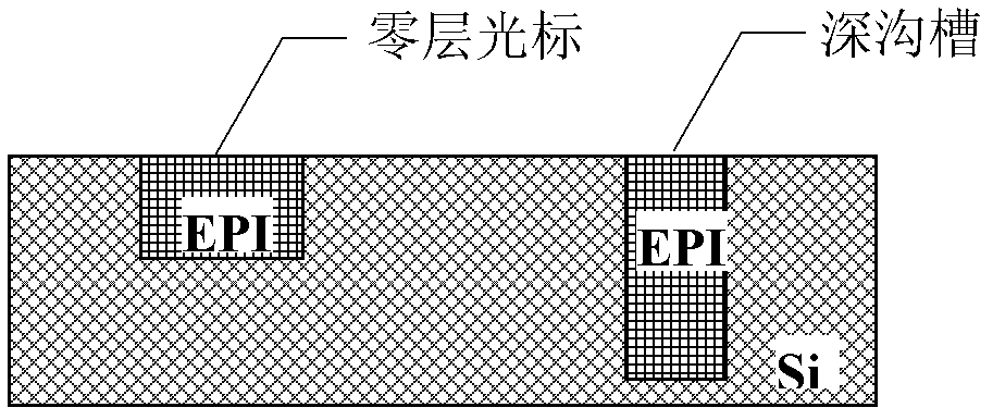
[0035] The present invention makes the method for the zero-layer lithography mark of the high-voltage device without barrier layer, comprises the following steps:

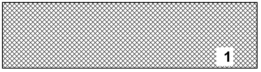
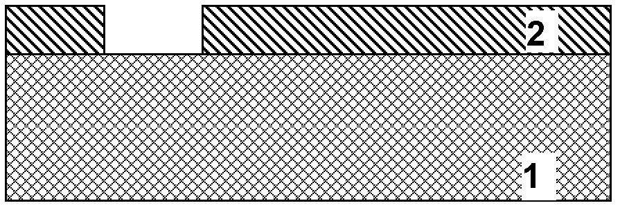
[0036] The first step, in the figure 2 A layer of photoresist 2 is formed on the silicon substrate 1 shown, and exposure and development are carried out on the silicon substrate 1, as image 3 Shown; Then etch out the zero-layer photolithography mark groove on the silicon substrate 1, as Figure 4 As shown; the depth of the zero-layer lithographic marking groove is 0.1-10 microns, the width is 1-10 microns, and the length is 1-10 microns; the shape of the groove can be vertical or inclined;

[0037] The size of the zero-layer lithography marking groove is preferably: 0.5-5 microns in depth, 1-6 microns in width, and 1-10 microns in length;

[0038] In the second step, the photoresist 2 on the silicon substrate 1 is removed, such as Figure 5 Shown; Then a layer of dielectric layer 3 is deposited on the silicon ...


PUM

PropertyMeasurementUnit
thicknessaaaaaaaaaa
depthaaaaaaaaaa
widthaaaaaaaaaa

Abstract

The invention discloses a method for producing zero layer photoetching marking of a high-voltage device without barrier layers. The method for producing the zero layer photoetching marking of the high-voltage device without the barrier layers comprises the following steps: (1) etching a zero layer lithography marking groove, (2) depositing a layer of medium layer and removing medium layers of regions outside the zero layer lithography marking groove, (3) etching a deep groove, (4) selectively growing an epitaxial layer on a silicon substrate, (5) removing anti-configuration epitaxial materials deposited on the silicon substrate in the epitaxial growth process of epitaxial layer, (6) etching away a medium layer inside the zero layer lithography marking groove by the adoption of the method of wet etching and leaving a zero layer lithography marking graph. Through the method for producing the zero layer photoetching marking of the high-voltage device without the barrier layers, lithography markings which are easy to recognize can be formed on the high-voltage device without the barrier layers, and therefore a follow-up film layer can be directed at conveniently, smooth of technological process can be guaranteed, and good yield of a product is improved.

Description

technical field [0001] The invention relates to a semiconductor process method, in particular to a method for making a zero-layer photolithography mark of a high-voltage-resistant device without a barrier layer. Background technique [0002] In today's semiconductor power applications, a new type of semiconductor device has emerged that can both increase the breakdown voltage and reduce the resistance in the on-state. It has alternately arranged PN column layers, which function as a super junction as a drift layer. [0003] The method of etching and filling deep trenches in the manufacturing process of super junction MOS transistors is to grow a layer of n-type epitaxial layer (single crystal silicon) on the n+ type silicon substrate, and then deposit a layer or Several layers of oxide film or nitride film, etch the deep trench, and fill the deep trench with p-type single crystal silicon for selective epitaxy, and finally use chemical mechanical polishing (CMP) process to p...

Claims


Application Information

Patent Timeline
Patent Type & Authority Applications(China)
IPC IPC(8): H01L21/311G03F7/20
Inventor 钱志刚季伟
Owner SHANGHAI HUAHONG GRACE SEMICON MFG CORP
Why Eureka
Try Eureka