Surface plasma wave demultiplexer based on destructive interference

A technology of surface plasmon and decomposition multiplexer, which is applied in the direction of instruments, optical waveguides, light guides, etc., can solve the problems of low transmission efficiency, achieve high transmission efficiency, solve reflection problems, and simple structure

Inactive Publication Date: 2013-04-17
XI'AN INST OF OPTICS & FINE MECHANICS - CHINESE ACAD OF SCI
View PDF2 Cites 13 Cited by
  • Summary
  • Abstract
  • Description
  • Claims
  • Application Information

AI Technical Summary

Problems solved by technology

[0005] The present invention provides a surface plasmon wave demultiplexer based on interference cancellation, which mainly solves the problem of low transmission efficiency of the existing surface plasmon wave demultiplexer

Method used


Image

  • Surface plasma wave demultiplexer based on destructive interference
  • Surface plasma wave demultiplexer based on destructive interference
  • Surface plasma wave demultiplexer based on destructive interference

Examples


Embodiment Construction

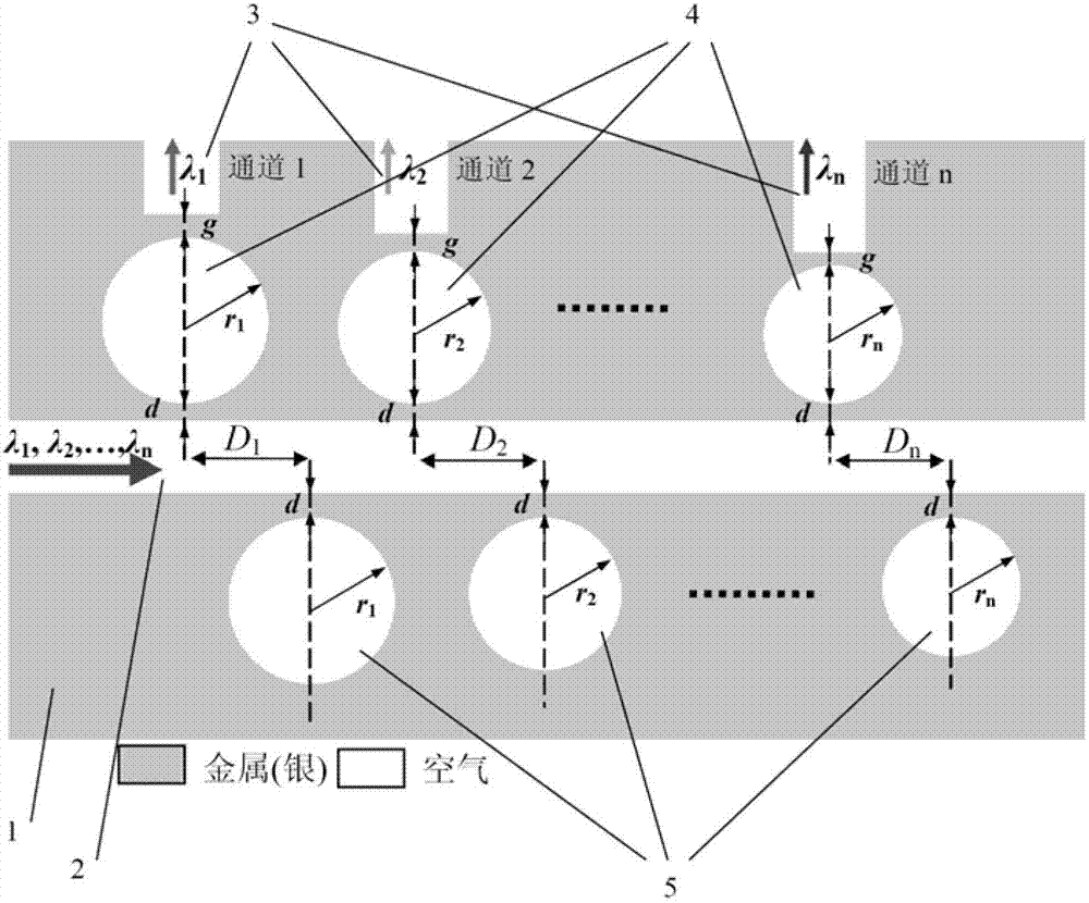
[0025] The surface plasmon wave demultiplexer based on interference cancellation of the present invention is mainly composed of a metal (silver) layer, a main waveguide, an exit channel, a coupling output resonant cavity, and a reflection resonant cavity. For details, see figure 1 .

[0026] The metal layer (slab) can be produced by using a laser molecular beam crystal epitaxial growth system. The main waveguide and resonant cavity can be obtained by etching the metal plate by using focused ion beam etching technology. The optical signal is introduced into the main waveguide through the coupling silicon waveguide or tapered optical fiber. When the optical signal is coupled out of the resonant cavity, because the coupling distance is smaller than the skin depth of the metal (the coupling distance d between the resonant cavity and the main waveguide is 10 nanometers, the coupling output resonance The coupling distance g between the cavity and the outgoing channel is 15 nanomete...


PUM


Abstract

The invention provides a surface plasma wave demultiplexer based on destructive interference, which mainly solves the problem that the transmission efficiency of the existing surface plasma wave demultiplexer is lower. The surface plasma wave demultiplexer based on the destructive interference comprises metal layers arranged at two sides of a medium layer; a plurality of coupled output resonant cavities are formed in the metal layer at one side of the medium layer; each coupled output resonant cavity is correspondingly provided with an outgoing channel; each outgoing channel is arranged at one side of the metal layer away from the medium layer and is symmetrical to the center of the coupled output resonant cavity. The structure of the surface plasma wave demultiplexer provided by the invention has stronger effects of light bondage, can break through the limitation of diffraction limit, and can transmit light in a nanometer scale; the surface plasma wave demultiplexer can be effectively connected with electronic apparatuses and conventional photon devices in a matching way, so that the reflection problem of the optical signal is effectively solved, and the surface plasma wave demultiplexer has wide application prospects in optical communication, optical integration, optical information processing and the like.

Description

technical field [0001] The invention relates to a wave demultiplexer, in particular to a surface plasmon wave demultiplexer based on interference and cancellation. Background technique [0002] The plasmonic wave demultiplexer has many advantages, such as simple and compact structure, small size, not limited by the diffraction limit, and provides the possibility of compatibility between electronic circuits and photonic devices. In many fields, especially optical integration, optical computing and optical It has broad application prospects in information processing and other fields. [0003] Based on the characteristics of metal nano-resonator filtering and high beam confinement of metal-dielectric-metal waveguide, surface plasmon wave demultiplexer has many unique advantages. Generally speaking, the position and transmission efficiency of the working wavelength can be effectively adjusted by rationally designing the geometric parameters of the metal resonator, and the optic...

Claims


Application Information

Patent Timeline
Patent Type & Authority Applications(China)
IPC IPC(8): G02B6/122G02B6/12
Inventor 刘雪明陆华王国玺
Owner XI'AN INST OF OPTICS & FINE MECHANICS - CHINESE ACAD OF SCI
Why Eureka
Try Eureka