
Photomask structure and manufacturing method thereof

A manufacturing method and technology of photolithography plate, which is applied in the direction of optics, photographic plate-making process of pattern surface, and original parts for photomechanical processing, etc., can solve the problems of increased transmittance, decreased phase shift value, high monitoring cost, etc.

Inactive Publication Date: 2013-04-17
SHANGHAI INTEGRATED CIRCUIT RES & DEV CENT
View PDF5 Cites 2 Cited by
  • Summary
  • Abstract
  • Description
  • Claims
  • Application Information

AI Technical Summary

Problems solved by technology

[0003] In order to prevent the decrease of the yield of silicon wafers caused by the crystalline defects of the lithography plate, in the integrated circuit manufacturing process, the lithography plate must be regularly scanned for defects to monitor the growth of crystal defects. Due to the large number of lithography plates and frequent use, the defect detection The cost of scanning and monitoring is very high; in addition, when defects are scanned, the photoresist plate must be sent back to the photoresist plate manufacturer for cleaning to remove crystal defects. This cleaning will cause damage to the surface pattern of the photoresist plate, especially for The phase shift layer on the surface of the phase shift photoresist plate, due to the increase in the number of cleanings, leads to a decrease in the thickness of the phase shift layer, and the decrease in the thickness of the phase shift layer will lead to a decrease in the phase shift value and an increase in the transmittance. When the phase shift value and the transmittance Exceeding the specifications will directly cause the photolithography plate to be scrapped

Method used


Image

  • Photomask structure and manufacturing method thereof
  • Photomask structure and manufacturing method thereof
  • Photomask structure and manufacturing method thereof

Examples


Embodiment 1

[0033] now attached image 3 , 4 , a preferred embodiment of a photoresist plate structure and its manufacturing method of the present invention will be described in detail.

[0034] image 3 It is a schematic diagram of the preparation process of a preferred embodiment of the method for manufacturing a photolithography plate structure of the present invention; Figure 4 It is a schematic diagram of specific preparation steps of a method for manufacturing a photoresist plate structure according to the above-mentioned preferred embodiment of the present invention.

[0035] see Figure 4 c, a photoresist structure in this embodiment includes: a glass substrate 41, a photoresist pattern 42 on the glass substrate 41, a transparent protective layer 43 covering the photoresist pattern 42, and a transparent protective layer located on the transparent protective layer. The mask film 44 above the layer 43, the mask film 44 covers the photoresist pattern 42 area. In the present inv...

Embodiment 2

[0041] now attached Figure 5 , 6 , another preferred embodiment of a photoresist plate structure and its manufacturing method of the present invention will be described in detail.

[0042] Figure 5 It is a schematic diagram of the preparation process of another preferred embodiment of the method for manufacturing a photolithography plate structure of the present invention; Image 6 It is a schematic diagram of specific preparation steps of a method for manufacturing a photoresist plate structure according to another preferred embodiment of the present invention.

[0043] see Image 6c, a photoresist structure in this embodiment includes: a glass substrate 61, a photoresist pattern 62 on the glass substrate 61, a transparent protective layer 63 covering the photoresist pattern 62, and a transparent protective layer located on the transparent protective layer. The mask film 64 above the layer 63, the mask film 64 covers the photoresist pattern 62 area. In the present inve...


PUM


Abstract

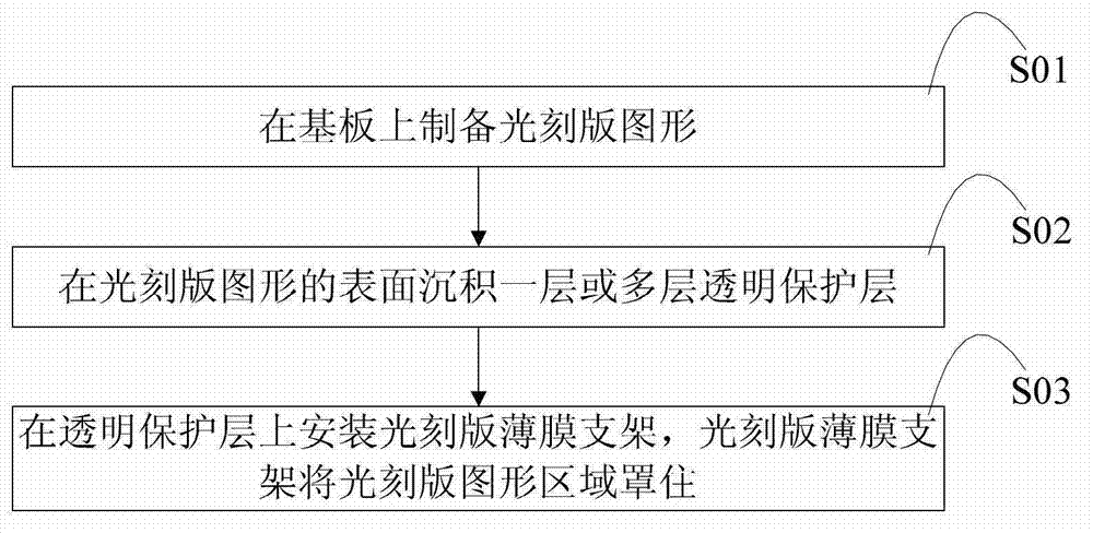
The invention provides a photomask structure which comprises a substrate, a photomask pattern positioned on the surface of the substrate, one or multiple transparent protective layers covering the surface of the photomask pattern, and a mask film arranged above the transparent protective layer(s), wherein the mask film covers a region of the photomask pattern; and the invention further provides a manufacturing method of the above photomask structure, wherein the manufacturing method comprises the following steps: preparing the photomask pattern on the surface of the substrate; forming one or multiple transparent protective layers on the surface of the photomask pattern; and mounting the mask film on the substrate. According to the invention, one or multiple transparent protective layers is / are deposited on the surface of the photomask pattern, so that the photomask pattern can be protected, and the crystallographic defects formed on the surface of the photomask pattern can be reduced and avoided, so that the projection accuracy and the yield of the photomask are improved, the repair rate of the photomask is reduced, and the service life of the photomask is prolonged.

Description

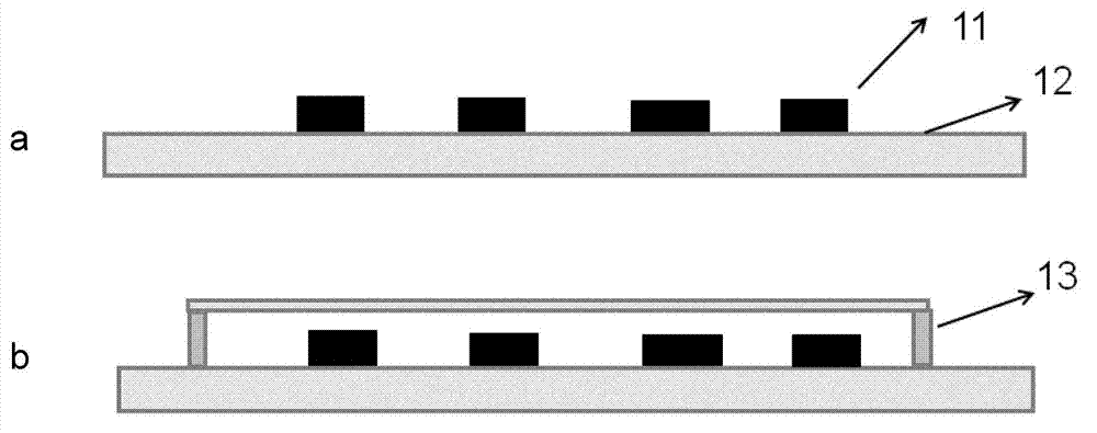
technical field [0001] The invention relates to the technical field of integrated circuit manufacturing, in particular to a photolithography plate structure and a manufacturing method thereof. Background technique [0002] The problem of crystalline defects in photolithographic plates has always been a major problem in the field of integrated circuits. As the photoresist plate is used more often and the photoresist plate is stored longer, crystal defects will grow on the surface of the photoresist plate, and the longer it is, the more crystal defects will directly cause the normal pattern of the photoresist plate projected on the silicon wafer to occur. Defects lead to lower yields. Please refer to the photoresist plate structure in the prior art figure 2 b, generally includes a substrate, a photoresist pattern 11 on the substrate 12, and a mask 13. figure 1 It is a schematic diagram of the preparation process of the manufacturing method of the photoresist plate structur...

Claims


Application Information

Patent Timeline
IPC IPC(8): G03F1/48
Inventor 袁伟
Owner SHANGHAI INTEGRATED CIRCUIT RES & DEV CENT
Learn More