Field emission electron source and preparation method of carbon nanotube graphene composite structure thereof

A graphene composite and field emission technology, applied in the manufacture of discharge tubes/lamps, components of discharge tubes/lamps, nanotechnology, etc., can solve problems such as poor electrical conductivity, low total emission current, and poor emission stability , to achieve the effects of improving emission capability and stability, high emission current density, and efficient and stable emission current

Active Publication Date: 2013-04-17
广州市昊志影像科技有限公司
View PDF6 Cites 26 Cited by
  • Summary
  • Abstract
  • Description
  • Claims
  • Application Information

AI Technical Summary

Problems solved by technology

[0006] In view of the above-mentioned prior art, the object of the present invention is to provide a field emission electron source of a carbon nanotube graphene composite structure, which aims to solve the emission stability of the existing field emission electron source field emission cathode array. Poor performance, low total emission current, and thermal contact resistance between the field emitter and the substrate, and the large contact resistance leads to poor thermal and electrical conductivity

Method used


Image

  • Field emission electron source and preparation method of carbon nanotube graphene composite structure thereof
  • Field emission electron source and preparation method of carbon nanotube graphene composite structure thereof
  • Field emission electron source and preparation method of carbon nanotube graphene composite structure thereof

Examples


Embodiment Construction

[0042] The present invention will be further described below in conjunction with the drawings and specific implementations.

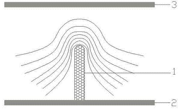
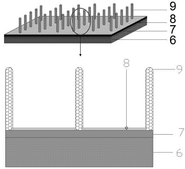
[0043] A field emission electron source with a carbon nanotube graphene composite structure, comprising a conductive substrate, a graphene film layer, and a carbon nanotube array oriented perpendicular to the graphene film layer, the graphene film layer being adhered to the conductive substrate One end of the carbon nanotubes in the carbon nanotube array is connected with the graphene film layer to form an integral structure. The diameter of the carbon nanotube is 1 nm-100 nm. The graphene film layer is a multilayer or a single layer. The conductive substrate is a metal substrate or other materials covered with metal electrodes.

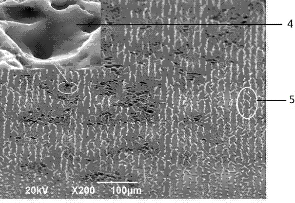
[0044] Using carbon nanotube bundles with a diameter of 100nm~100μm as the emission unit, or a microcarbon nanotube with a width of 100nm~100μm, it is easy to achieve directional growth, can obtain a stable large emission current...


PUM

PropertyMeasurementUnit
diameteraaaaaaaaaa
diameteraaaaaaaaaa
diameteraaaaaaaaaa

Abstract

The invention discloses a field emission electron source and a preparation method of a carbon nanotube graphene composite structure thereof. The field emission electron source comprises a conductive substrate, a graphene film layer and a carbon nanotube array which is directionally perpendicular to the graphene film layer, wherein the graphene film layer is adhered onto the conductive substrate, and one end of each carbon nanotube in the carbon nanotube array is connected with the graphene film layer to form an integrated structure. The emission capacity and stability of the carbon nanotube array field emission electron source are greatly improved, so that the electron source obtains highly efficient and stable emission current, and can bear extremely high emission current density.

Description

Technical field [0001] The invention relates to the technical field of vacuum electronics, in particular to a field emission electron source and a method for preparing a carbon nanotube graphene composite structure. Background technique [0002] Vacuum electronic devices are now showing a rapid development trend, and the market demand is increasing day by day, especially miniaturized vacuum electronic devices and integrated vacuum electronic devices are the current development focus. The field emission electron source works at low temperature or room temperature. Compared with the thermionic source in the current electric vacuum device, it has the advantages of high brightness, low power consumption, small energy scattering, fast response speed and no thermal evaporation, so it is used as a vacuum electronic device The electron source can greatly improve the performance of vacuum electronic devices. [0003] The schematic diagram of the field emission cathode electron source is as...

Claims


Application Information

Patent Timeline
Patent Type & Authority Applications(China)
IPC IPC(8): H01J1/304H01J9/02B82Y30/00B82Y40/00
Inventor 陈泽祥王智慧唐宁江
Owner 广州市昊志影像科技有限公司
Why Eureka
Try Eureka