
Optical module debugging system

A technology for debugging systems and optical modules, applied in transmission systems, electromagnetic wave transmission systems, electrical components, etc., can solve problems such as a lot of capital, cost, and high cost, and achieve the goal of reducing debugging costs, saving warm-up time, and improving debugging efficiency. Effect

Active Publication Date: 2013-04-17
HISENSE BROADBAND MULTIMEDIA TECH
View PDF6 Cites 16 Cited by
  • Summary
  • Abstract
  • Description
  • Claims
  • Application Information

AI Technical Summary

Problems solved by technology

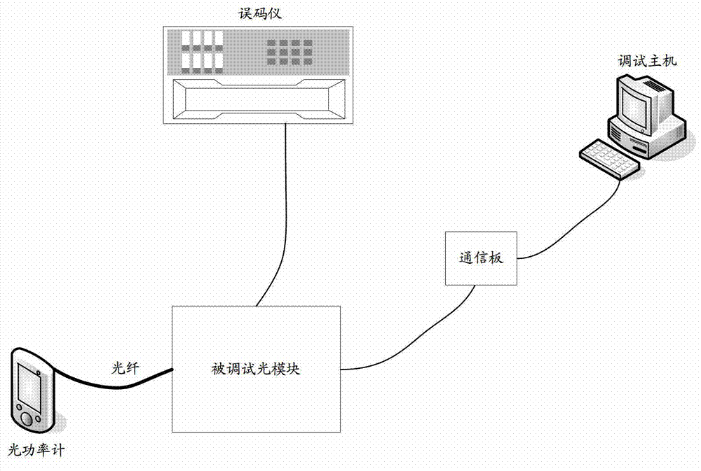
[0014] Because the debugging method of the prior art needs to adopt more expensive equipment such as a bit error meter and an optical power meter, a large amount of funds and costs need to be invested in mass production and debugging of the production line of the optical module; therefore, the optical module of the prior art Debugging systems and debugging methods has a high cost

Method used


Image

  • Optical module debugging system
  • Optical module debugging system
  • Optical module debugging system

Examples


Embodiment Construction

[0042] In order to make the object, technical solution and advantages of the present invention clearer, the present invention will be described in further detail below with reference to the accompanying drawings and preferred embodiments. However, it should be noted that many of the details listed in the specification are only for readers to have a thorough understanding of one or more aspects of the present invention, and these aspects of the present invention can be implemented even without these specific details.

[0043] As used herein, terms such as "module" and "system" are intended to include computer-related entities such as, but not limited to, hardware, firmware, a combination of hardware and software, software, or software in execution. For example, a module may be, but is not limited to being limited to being, a process running on a processor, a processor, an object, an executable, a thread of execution, a program, and / or a computer.

[0044] The technical solution...


PUM


Abstract

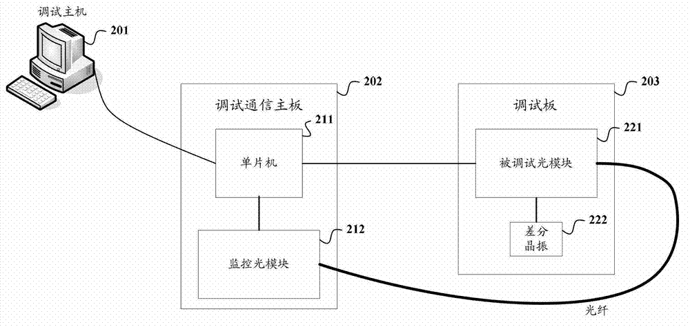
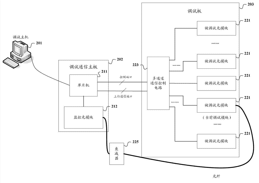
The invention discloses an optical module debugging system, which comprises a debugging board, a debugging communication mainboard and a debugging host machine, wherein the debugging board comprises a differential crystal oscillator which is used for providing data electric signals for a debugged optical module arranged on the debugging board, the debugging communication mainboard comprises a single chip microcomputer and a monitoring optical module, the monitoring optical module detects optical signals emitted by the debugged optical module after the data electric signals are received through a photodiode, and in addition, the response current generated by the photodiode is detected, the debugging host machine is used for being communicated with the single chip microcomputer and obtains the response current detected by the monitoring optical module through the single chip microcomputer, the optical power is calculated according to the obtained response current, the bias current in the debugged optical module is regulated through the single chip microcomputer according to the calculated optical power, and the optical power is debugged. The monitoring optical module is adopted for replacing an optical power meter for testing the optical power of laser emitted by the debugged optical module, and the differential crystal oscillator capable of outputting high-frequency differential electric signals is adopted for replacing an error detector, so the debugging cost of the optical module is greatly reduced.

Description

technical field [0001] The invention relates to optical fiber communication technology, in particular to an optical module debugging system. Background technique [0002] Recently, the optical communication market is in a stage of rapid development. With the maturity of technology and the market's demand for bandwidth, optical fiber communication systems have begun to be applied on a large scale and gradually entered thousands of households. The optical module for photoelectric conversion is the core component of the optical fiber communication system, which is used in various devices in the optical fiber communication system, such as OLT (Optical Line Terminator, optical line terminal), ONU (optical net unit, optical network unit) , Optical transceiver, etc. [0003] Before the optical module leaves the factory and is installed in the optical fiber communication system, it needs to go through the debugging process. The debugging process of the optical module is carried ou...

Claims


Application Information

Patent Timeline
Patent Type & Authority Applications(China)
IPC IPC(8): H04B10/073
Inventor 葛君张华
Owner HISENSE BROADBAND MULTIMEDIA TECH
Learn More