Device and method for laser etching of conducting film layers on touch on lens (TOL) and one glass solution (OGS) touch components

A conductive film layer, laser etching technology, applied in laser welding equipment, welding equipment, metal processing equipment and other directions, can solve the problems of limited application field, large initial investment, increased labor cost and production cost, etc., to achieve linear stability, functional Complete, simple processing results

Inactive Publication Date: 2013-04-24
SUZHOU DELPHI LASER
View PDF7 Cites 10 Cited by
  • Summary
  • Abstract
  • Description
  • Claims
  • Application Information

AI Technical Summary

Problems solved by technology

However, the yellow photolithography process requires a large initial investment and high cost. The selectivity of materials is relatively narrow, and it needs to be matched with different photoresists. It is not suitable for all conductive film production methods on the market. In addition, the daily maintenance cost is relatively high. , the cost of consumables and labor brings an increase in the entire production cost, and the application field is more restricted

Method used


Image

  • Device and method for laser etching of conducting film layers on touch on lens (TOL) and one glass solution (OGS) touch components

Examples


Embodiment Construction

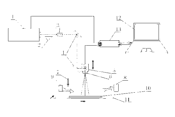
[0020] like figure 1 As shown, the device used for laser etching of the conductive film layer on TOL and OGS touch includes a laser 1, a shutter 2, a beam expander 3, a full-reflection lens group 4, a vibrating mirror system 5, and a telecentric field mirror 6 , the laser 1 is a laser with a wavelength of 199nm to 1064nm, a pulse width of 1ps to 500ns, and a frequency of 1KHz to 2MKHz. The output end of the beam mirror 3 is arranged with a full reflection mirror group 4, and the output end of the full reflection mirror group 4 is arranged with a galvanometer system 5 and a telecentric field mirror 6 in turn, and the output end of the telecentric field mirror 6 is facing the vacuum adsorption platform 11, A CCD alignment observation system 7 is arranged above the vacuum adsorption platform 11, an air blowing system 9 is arranged on one side of the vacuum adsorption platform 13, and a dust collection system 8 is installed on the other side; the laser 1 and the vibrating mirror s...


PUM

PropertyMeasurementUnit
wavelengthaaaaaaaaaa

Abstract

The invention relates to a device and a method for laser etching of conducting film layers on touch on lens (TOL) and one glass solution (OGS) touch components. Lasers emitted by a laser enter a beam expanding lens through an optical shutter, light beams enter a total reflection lens group to be subjected to light path adjustment after beam expansion and collimation are performed to the light beams through the beam expanding lens, the lasers are totally reflected to a galvanometer system and accurately controlled by a telecentric field lens to focus to a conducting film on glass, and the size of each focus light spot is 20-40 mu m; the laser and the galvanometer system are in data communication with an industrial personal computer through a communication system so as to transform scanning patterns to digital signals, the patterns are transformed onto a work piece to be etched and processed, and the work piece to be processed is adsorbed by a vacuum adsorption platform; a charge coupled device (CCD) alignment observation system shoots leading-in localizers and grasps targets to control processing; and after one unit is etched by the lasers, the vacuum adsorption platform moves the next unit, the lasers start to perform processing again, and such is repeated so that etching of processing breadth is achieved. The processing way is concise, the processing efficiency is high, and consumable items are not required.

Description

technical field [0001] The invention relates to a device and method for laser etching conductive film layers on TOL and OGS touch controls, and belongs to the technical field of laser micromachining. Background technique [0002] OGS (One glass solution) structure: ITO conductive film and sensor are directly formed on the protective glass, and a piece of glass plays the dual role of protective glass and touch sensor at the same time. The advantages of OGS are: 1) save the cost of a layer of glass and reduce the cost of a lamination; 2) reduce the weight; 3) increase the light transmittance. OGS can better meet the needs of ultra-thin smart terminals and improve the display effect. It is an inevitable choice for high-end brand terminals in the future. The TOL (Touch On Lens) solution is a solution in the specific technical evolution direction of OGS, that is, the touch module is integrated with the upstream strengthened glass Cover Lens, and the touch module is made on the C...

Claims


Application Information

Patent Timeline
Patent Type & Authority Applications(China)
IPC IPC(8): B23K26/36B23K26/16B23K26/42B23K26/06B23K26/064B23K26/362B23K26/70
Inventor 赵裕兴狄建科蔡仲云
Owner SUZHOU DELPHI LASER
Why Eureka
Try Eureka