Preparation method based on Ni membrane annealing for SiC substrate side grid graphene transistor

A graphene and transistor technology, applied in the field of microelectronics, can solve the problems of decreased mobility of top-gate TG-GFETs, easily damaged graphene films, and high energy consumption, so as to avoid device performance degradation and avoid carrier migration. The effect of reducing the rate and improving the safety

Inactive Publication Date: 2013-05-01
XIDIAN UNIV
View PDF3 Cites 2 Cited by
  • Summary
  • Abstract
  • Description
  • Claims
  • Application Information

AI Technical Summary

Problems solved by technology

The main disadvantages of this method are: complex process, special removal of catalyst is required, large energy consumption and high production cost
They all have certain disadvantages, but this will not affect the application prospects of graphene in field effect transistors
In the existing preparation process of graphene field effect transistor GFET, graphene ne...

Method used


Image

  • Preparation method based on Ni membrane annealing for SiC substrate side grid graphene transistor
  • Preparation method based on Ni membrane annealing for SiC substrate side grid graphene transistor
  • Preparation method based on Ni membrane annealing for SiC substrate side grid graphene transistor

Examples


Embodiment 1

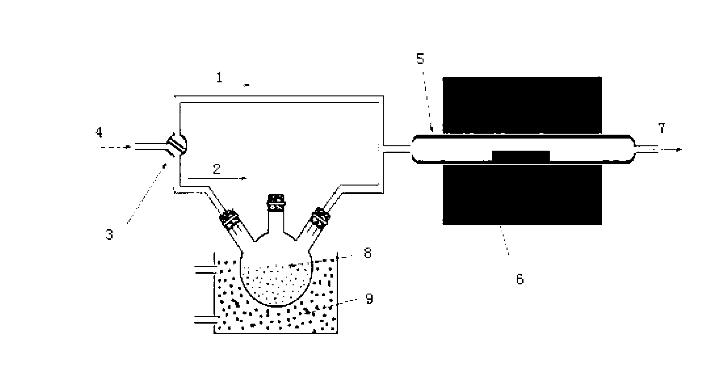
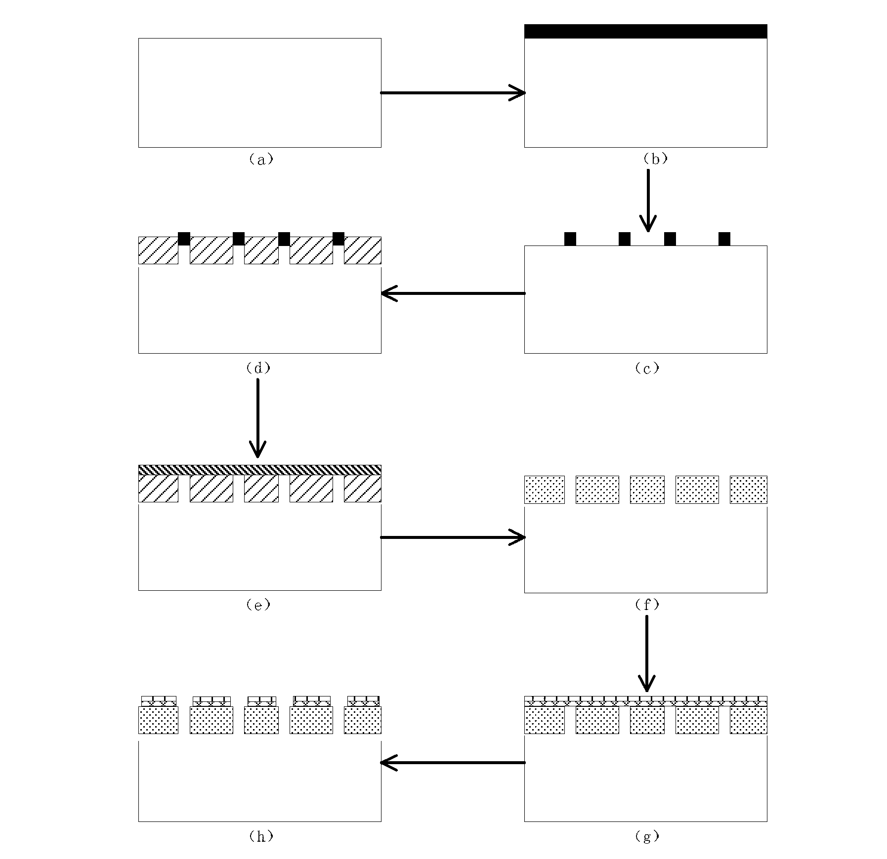
[0034] refer to figure 2 , the present invention makes the step of connection type side-gate graphene transistor as follows:

[0035] Step 1: Wash the 6H-SiC sample to remove surface contaminants such as figure 2 (a).

[0036] (1.1) Use NH for 6H-SiC samples 4 OH+H 2 o 2 Soak the sample in the reagent for 10 minutes, take it out and dry it to remove the organic residue on the surface of the sample;

[0037] (1.2) Use HCl+H on the 6H-SiC sample after removing the surface organic residues 2 o 2 The reagent soaked the sample for 10 minutes, took it out and dried it to remove ionic contamination.

[0038]Step 2: Deposit a layer of SiO on the surface of the 6H-SiC sample 2 ,Such as figure 2 (b).

[0039] (2.1) Put the cleaned 6H-SiC sample into the plasma-enhanced chemical vapor deposition PECVD equipment system, adjust the internal pressure of the system to 3.0Pa, adjust the radio frequency power to 100W, and adjust the temperature to 150°C;

[0040] (2.2) Introduce ...

Embodiment 2

[0069] refer to Figure 4 , the present invention makes the steps of the non-connected side-gate graphene transistor as follows:

[0070] Step 1: Clean the 4H-SiC sample to remove surface contaminants such as Figure 4 (a).

[0071] Use NH for 4H-SiC samples 4 OH+H 2 o 2 Soak the sample in the reagent for 10 minutes, take it out and dry it to remove the organic residue on the surface of the sample; use HCl+H 2 o 2 The reagent soaked the sample for 10 minutes, took it out and dried it to remove ionic contamination.

[0072] Step 2: Deposit a layer of SiO on the surface of the 4H-SiC sample 2 ,Such as Figure 4 (b).

[0073] Put the cleaned 4H-SiC sample into the plasma-enhanced chemical vapor deposition PECVD equipment system, adjust the internal pressure of the system to 3.0Pa, adjust the radio frequency power to 100W, and adjust the temperature to 150°C; SiH at a flow rate of 30 sccm 4 , with a flow rate of 60 sccm of N 2 O and N at a flow rate of 200 sccm 2 ,, s...

Embodiment 3

[0096] refer to figure 2 , the present invention makes the step of connection type side-gate graphene transistor as follows:

[0097] Step A: Use NH on the 4H-SiC substrate substrate 4 OH+H 2 o 2 Soak the sample in the reagent for 10 minutes, take it out and dry it to remove the organic residue on the surface of the sample; use HCl+H 2 o 2 Soak the sample in the reagent for 10 minutes, take it out and dry it to remove ionic contaminants such as figure 2 (a).

[0098] Step B: Put the cleaned 4H-SiC sample into the plasma-enhanced chemical vapor deposition PECVD equipment system, adjust the internal pressure of the system to 3.0Pa, adjust the radio frequency power to 100W, and adjust the temperature to 150°C; SiH 4 , N 2 O and N 2 Three gases, of which SiH 4 The flow rate is 30 sccm, N 2 O flow rate is 60 sccm, N 2 The flow rate is 200sccm, making SiH 4 with N 2 O was reacted for 60 minutes to deposit a layer of SiO with a thickness of 0.8 μm on the surface of th...


PUM

PropertyMeasurementUnit
Thicknessaaaaaaaaaa

Abstract

The invention discloses a preparation method based on Ni membrane annealing for a SiC substrate side grid graphene transistor and mainly solves the problems of low graphene channel carrier mobility and carrier scattering caused by top grid dielectric of a graphene transistor prepared by the prior technology. The preparation method is implemented by the following steps that a SiC sample substrate is cleaned; a SiO2 layer is deposited on the surface of the SiC sample substrate, and a side grid pattern is formed on the SiO2 layer in a photo-etching manner; the photo-etched sample substrate is placed in a quartz tube, and a carbon membrane is generated through the reaction of gaseous CCl4 and SiC; then the sample substrate with the carbon membrane is placed in a buffer hydrofluoric acid solution to remove the SiO2; a Ni membrane is deposited on the carbon membrane of the sample substrate, and the sample substrate is placed in Ar gas for annealing, so graphene of a side grid is generated; and finally, a metal Pd/Au layer is deposited on the graphene sample substrate and is etched to form metal contacts of a side grid transistor. The side grid graphene transistor prepared by the preparation method has high carrier mobility and can effectively restrain the scattering effect, so that the modulation effect of the grid of the graphene transistor on the channel carrier concentration is improved.

Description

technical field [0001] The invention belongs to the technical field of microelectronics, and relates to a method for preparing a semiconductor device, in particular to a method for preparing a SiC substrate side-gate graphene transistor based on Ni film annealing. technical background [0002] As people's demand for high-performance, high-reliability, and low-power equipment increases, more and more attention is paid to the characteristics of devices on integrated circuits. Graphene, a material composed of a two-dimensional hexagonal carbon lattice, has been discovered since 2004 by two scientists, Andre Jem and Kostya Novo, from the University of Manchester, UK, due to its outstanding electrical structural properties. After Love discovered it, it was regarded as a candidate material for the manufacture of high-performance devices. [0003] The preparation method of existing graphene, as application number is 200810113596.0 " method for preparing graphene by chemical vapor ...

Claims


Application Information

Patent Timeline
IPC IPC(8): H01L21/335
Inventor 郭辉张晨旭张玉明张克基雷天民胡彦飞
Owner XIDIAN UNIV
Why Eureka
Try Eureka