Trimming resistor and preparation method thereof

A technology for trimming resistors and manufacturing methods, which is applied in semiconductor/solid-state device manufacturing, circuits, electrical components, etc. It can solve problems such as trimming failure, insufficient trimming, and increased test condition debugging, and achieves small and easy fusing areas. Trimming and solving the effect of excessive trimming

Active Publication Date: 2013-05-08
HANGZHOU SILAN INTEGRATED CIRCUIT
View PDF8 Cites 2 Cited by
  • Summary
  • Abstract
  • Description
  • Claims
  • Application Information

AI Technical Summary

Problems solved by technology

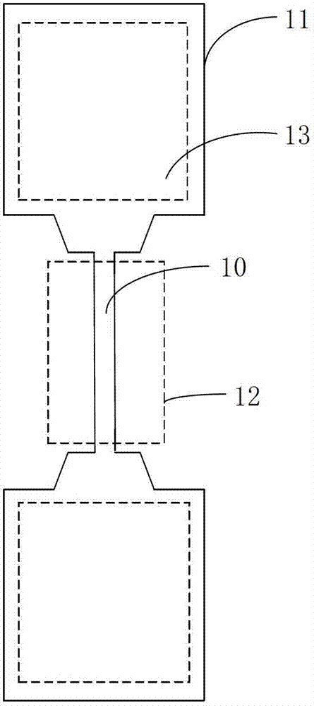
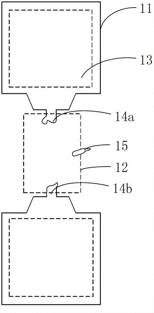
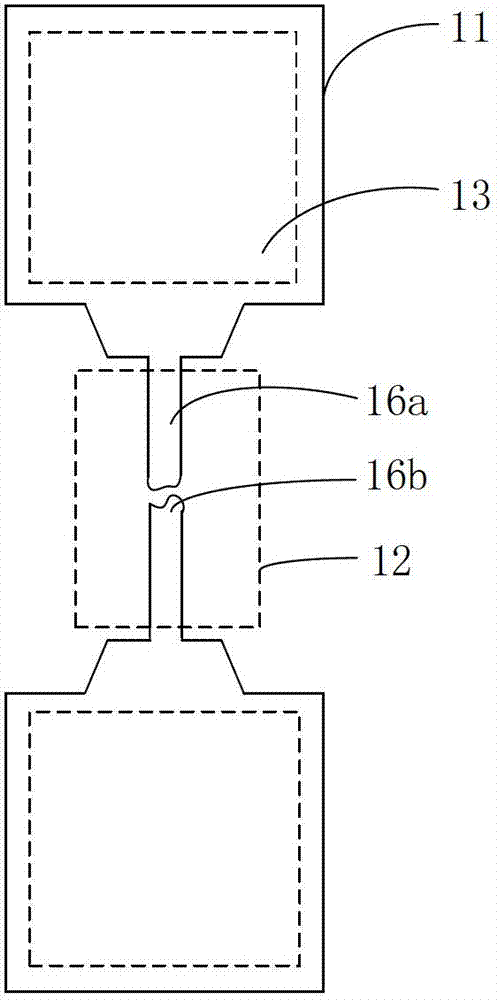
[0008] Therefore, in the traditional metal fuse trimming resistor, since any position of the entire trimming metal may become the most preferential fusing point during the trimming process, the trimming metal is prone to over-trimming and the entire metal is trimmed. , Insufficient repair and adjustment, and various situations of repair and adjustment failure; in addition, because the fusing point is not fix...

Method used


Image

  • Trimming resistor and preparation method thereof
  • Trimming resistor and preparation method thereof
  • Trimming resistor and preparation method thereof

Examples


Embodiment 1

[0079] See attached Figure 5 , combined with Figures 6 to 14 The process of the manufacturing method of the trimming resistor whose curved shape is a corner provided by the present invention is described in detail.

[0080] S1: Provide a semiconductor substrate, and fabricate a dielectric layer on the semiconductor substrate.

[0081] see Figure 6 , a semiconductor substrate 30 is provided, and a dielectric layer 31 is formed on the semiconductor substrate 30 .

[0082] Wherein, the semiconductor substrate 30 may be a silicon substrate, a silicon germanium substrate, a III-V group element compound substrate or other semiconductor material substrates known to those skilled in the art, and a silicon substrate is used in this embodiment. . More specifically, a MOS field effect silicon-containing material or a silicon compound may be formed in the semiconductor substrate 30 used in this embodiment. The semiconductor substrate provided for bipolar circuits is usually a P(11...

Embodiment 2

[0108] See attached Figure 5 , combined with Figures 16 to 26 The process of the manufacturing method of the trimming resistor whose bending shape is arc-shaped provided by the present invention is described in detail.

[0109] Step S1 in the present embodiment (referring to appended Figure 16 ) and step S2 (see attached Figure 17 ) Please refer to the content in steps S1 and S2 in the first embodiment, and details will not be repeated here.

[0110] The difference between this embodiment and the first embodiment lies in the difference between step S3 and step S4. The specific difference of step S3 is as follows:

[0111] see Figure 18 and Figure 19 , Figure 19 for Figure 18 In the top view of the front, the curved shape made in the area where the fuse is not removed has at least one arc 32a, so that the trimming structure with changing current density is formed, and the arc is made to have a radian θ is a circular or elliptical arc of 1-359 degrees, preferabl...

Embodiment 3

[0124] See attached Figure 5 , combined with Figures 27 to 32 The process of the manufacturing method of the trimming resistor with a curved shape having steps provided by the present invention will be described in detail.

[0125] Step S1 in the present embodiment (referring to appended Figure 27 ) Please refer to the content in step S1 in the first embodiment, which will not be repeated here.

[0126] The difference between this embodiment and the first embodiment lies in the difference of step S2, step S3 and step S4. The specific differences of step S2 are as follows:

[0127] see Figure 28 , before depositing the fuse 32, carry out processes such as photolithography and etching on the dielectric layer 31, and the etching stays in the dielectric layer 31, so that the dielectric layer 31 forms a shape with at least one step 31a, and The step height and the number of steps required by the dielectric layer 31 can be determined, and the number of steps 31a can be one,...


PUM

PropertyMeasurementUnit
Radianaaaaaaaaaa
Thicknessaaaaaaaaaa

Abstract

The invention provides a trimming resistor comprising a semiconductor substrate, a dielectric layer arranged on the semiconductor substrate, a fuse trimming shape arranged on the dielectric layer through deposit of a fuse, and a passivation layer, wherein the fuse trimming shape comprises a fusing area and two ends, a trimming structure capable of changing current density is arranged in the fusing area, and the two ends of the fuse trimming shape are respectively provided with connecting pads. The passivation layer is formed on the fuse trimming shape and the dielectric layer, and provided with a trimming window corresponding to the trimming structure and pressing point windows respectively corresponding to the connecting pads. The invention further provides a preparation method of the trimming resistor. Due to the fact that the fuse trimming shape is provided with the trimming structure capable of changing the current density in the fusing area, the effective cross section area of the fuse on the trimming structure is small, the current density is large, the fusing position is fixed, the fusing area is small, and meanwhile an opening of the trimming window on the fuse is small so as to reduce reliability risks caused by metal residue, chemical residue and the like due to the fact that the trimming window on the trimming resistor is too large.

Description

technical field [0001] The invention belongs to the technical field of semiconductor manufacturing technology, and in particular relates to a trimming resistor and a manufacturing method thereof. Background technique [0002] Integrated circuit layout design is usually relatively standardized and idealized. In the actual manufacturing process, it is affected by factors such as manufacturers, process methods, process fluctuations, and test conditions, resulting in errors in the expected dimensions and electrical functions of the design. For products that need to adjust the reference voltage and reference frequency, the current limiting and voltage dividing functions of resistors are widely used in analog circuits, but the resistance value is affected by the doping concentration and diffusion degree, and the error can reach ±20%. Such a large error Can not meet the requirements of high-precision circuits. In order to eliminate the impact of factors such as manufacturers, proc...

Claims


Application Information

Patent Timeline
IPC IPC(8): H01L23/525H01L21/768
Inventor 杨彦涛陈文伟刘慧勇韩健江宇雷雷辉
Owner HANGZHOU SILAN INTEGRATED CIRCUIT
Why Eureka
Try Eureka