Photoresist removal method and semiconductor production method

A technology of photoresist and deionized water, applied in semiconductor/solid-state device manufacturing, photosensitive material processing, electrical components, etc. Solve problems such as bottom silicon, achieve the effect of reducing photoresist residues, ensuring quality, and improving deglue efficiency

A technology of photoresist and deionized water, applied in semiconductor/solid-state device manufacturing, photosensitive material processing, electrical components, etc. Solve problems such as bottom silicon, achieve the effect of reducing photoresist residues, ensuring quality, and improving deglue efficiency

CN103107066AActive Publication Date: 2013-05-15CSMC TECH FAB2 CO LTD

Image

  • Photoresist removal method and semiconductor production method
  • Photoresist removal method and semiconductor production method
  • Photoresist removal method and semiconductor production method

Examples


Embodiment Construction

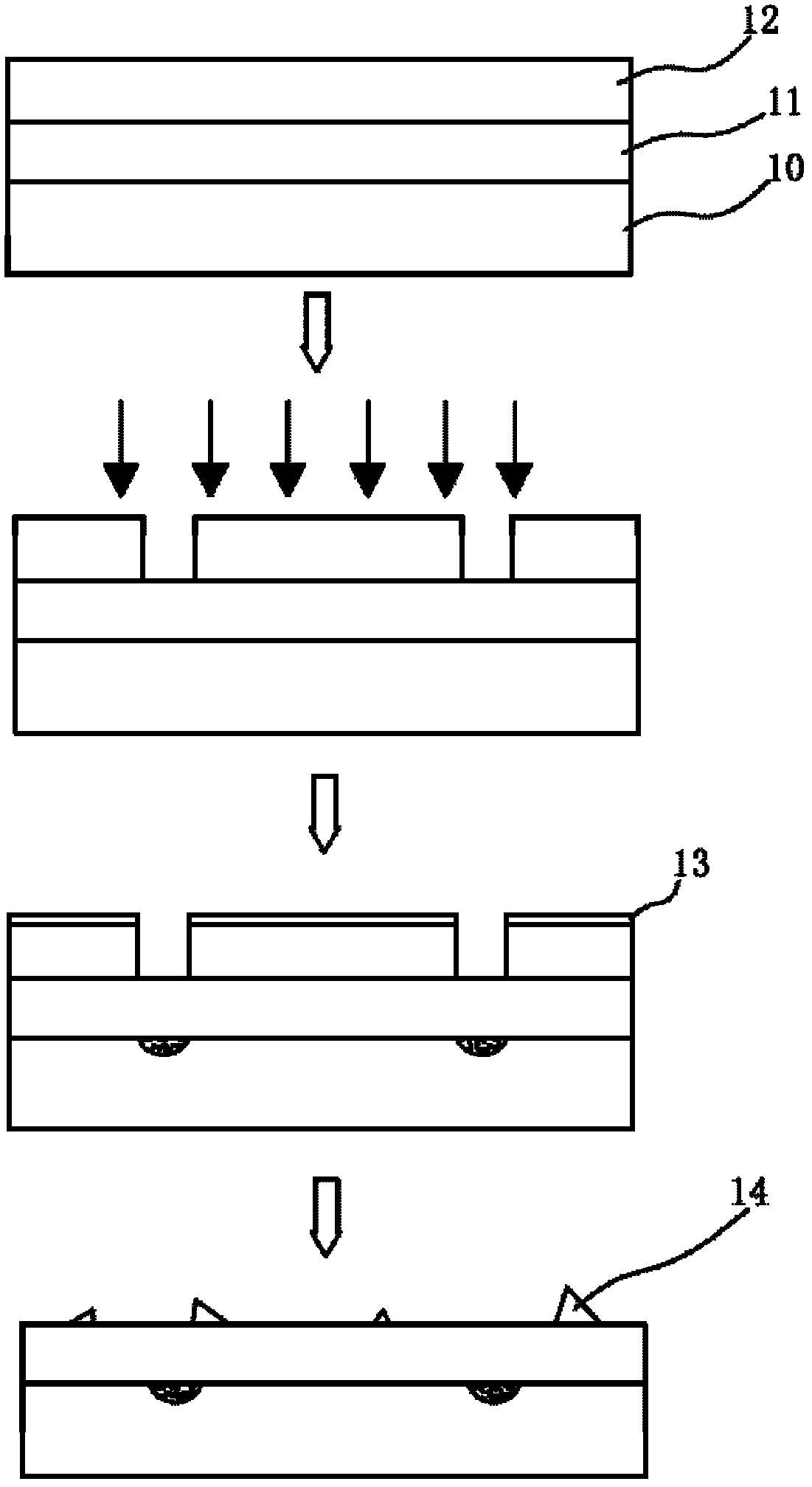
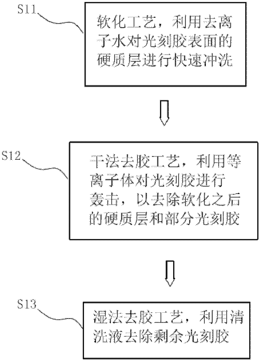
[0034] As mentioned in the background art, after the ion implantation process of the photoresist, a hard layer is formed due to the reaction of the surface with high-energy ions. The hard layer brings difficulties to the stripping process of the photoresist. In the existing degumming process, the plasma dry degumming process can remove part of the hard layer, but the plasma energy used is relatively large. When facing a process below 65nm, it is easy to damage the oxide layer as a buffer layer , thereby damaging the silicon substrate surface. However, the wet stripping process is difficult to effectively remove the hard layer, resulting in residual defects in the photoresist and affecting the quality of the device.

[0035] Therefore, the present invention proposes a method for removing the photoresist mask after the ion implantation process is performed using the photoresist as a mask during the manufacturing process of the semiconductor device.

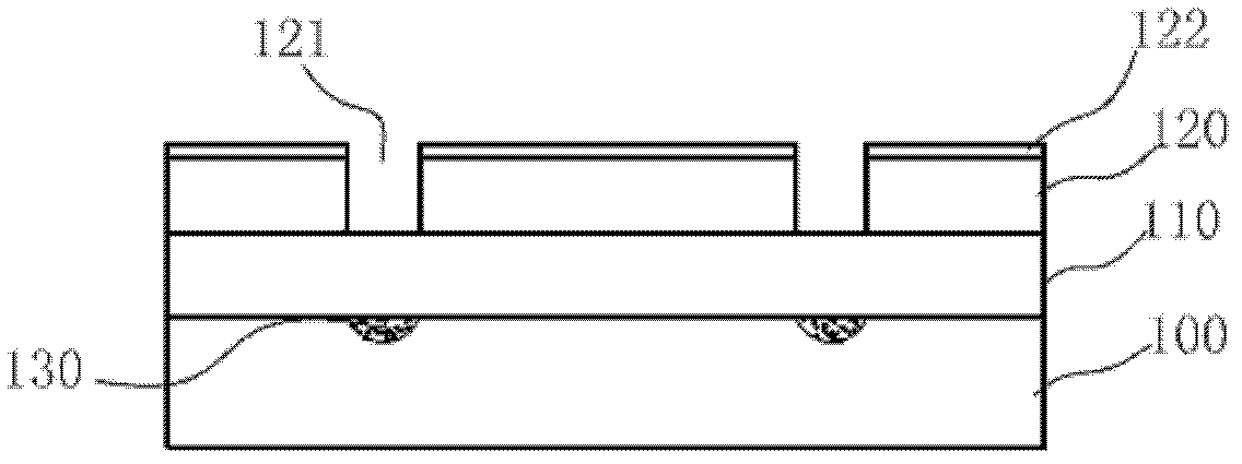
[0036] See figure 2 , ...


PUM

PropertyMeasurementUnit
thicknessaaaaaaaaaa

Abstract

The invention relates to a photoresist removal method and a semiconductor production method. The photoresist removal method is that after ions are injected into the art, the photoresist with a surface on which a hard layer is formed is removed. The method comprises the following steps: a softening process is used; a dry stripping process and a wet stripping process are used, due to the fact that the softening process is conducted on the hard layer of the surface of the photoresist, and the hard layer of the photoresist caused by the ion injection process and the like is softened, and thereby the removal of the photoresist is enabled to be simplified. Meanwhile the fact that the semi-conductive product is not damaged during the photoresist removal process is guaranteed, and the yield of the semi-conductive product is greatly improved. The invention further provides a semiconductor production method which comprises the photoresist removal method.

Description

technical field [0001] The invention relates to the field of semiconductor manufacturing, in particular to a method for removing photoresist after an ion implantation process. Background technique [0002] With the rapid development of semiconductor manufacturing technology, in order to achieve faster computing speed, larger data storage capacity and more functions of semiconductor devices, semiconductor wafers are developing towards higher component density and high integration. The feature size of CMOS devices has entered the nanometer stage, the gate width has become thinner and the length has become shorter than before. This makes the development of semiconductor devices produce two new requirements: low doping concentration control and ultra-shallow junction. [0003] Ion implantation overcomes the limitations of chemical diffusion processes, while also providing additional advantages. There is no lateral diffusion during the ion implantation process, the process is c...

Claims


Application Information

Patent Timeline
15 May 2013
Publication
CN103107066A
IPC
H01L21/027; G03F7/42
Inventors
陈亚威; 杨鑫