Metal bonding method of three-dimensional chip structure and bonding structure

A three-dimensional chip and metal bonding technology, which is applied in the manufacturing of electrical components, electric solid-state devices, semiconductor/solid-state devices, etc., can solve the problems of low reliability, complex process and high cost, achieve high reliability, simplify the process low cost effect

Active Publication Date: 2013-05-15
WUHAN XINXIN SEMICON MFG CO LTD
View PDF8 Cites 19 Cited by
  • Summary
  • Abstract
  • Description
  • Claims
  • Application Information

AI Technical Summary

Problems solved by technology

[0003] The technical problem to be solved by the present invention is to provide a metal bonding method and bonding structure of a three-dimensional chip structure to solve the problems of complex process, low reliability and high cost in the prior art

Method used


Image

  • Metal bonding method of three-dimensional chip structure and bonding structure
  • Metal bonding method of three-dimensional chip structure and bonding structure
  • Metal bonding method of three-dimensional chip structure and bonding structure

Examples


Embodiment Construction

[0037] The following is attached picture The principles and features of the present invention are described, and the examples given are only used to explain the present invention, and are not used to limit the scope of the present invention.

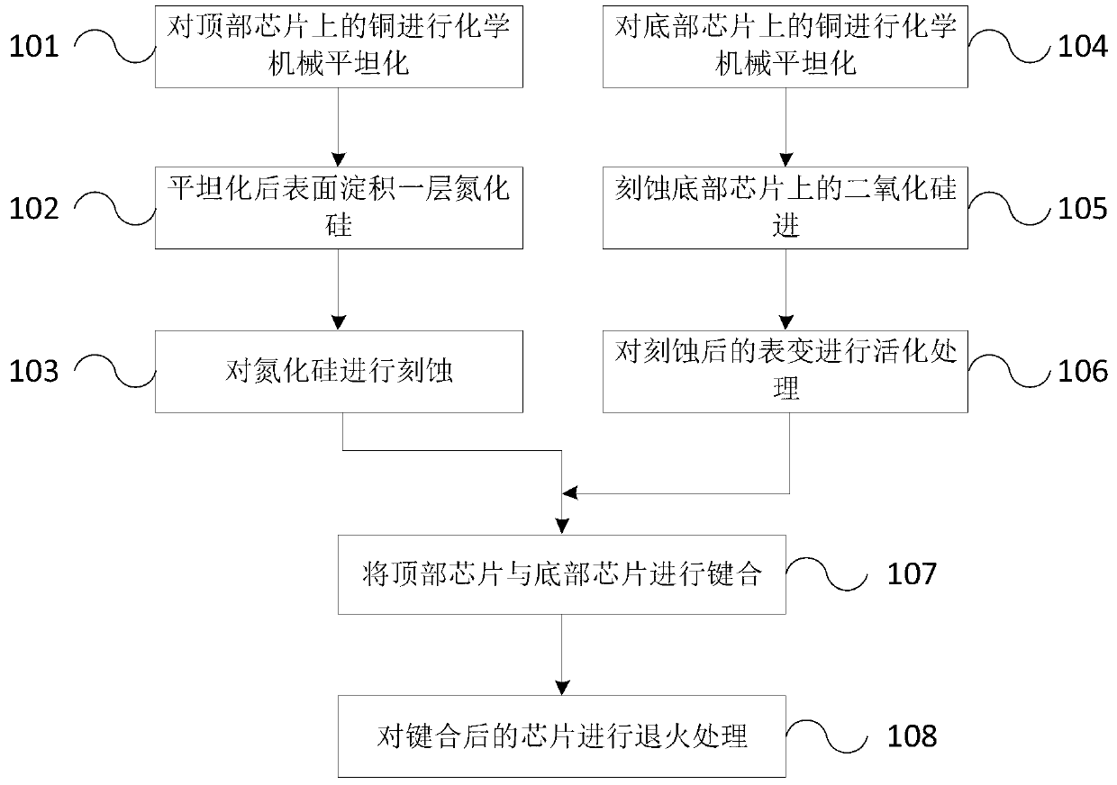
[0038] Such as figure 1 Shown, is the flow process of the inventive method picture , including the following steps:

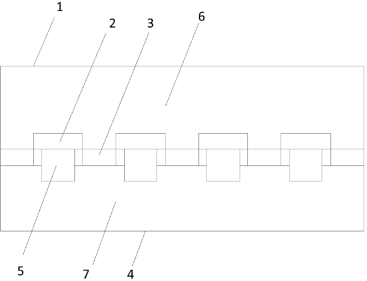
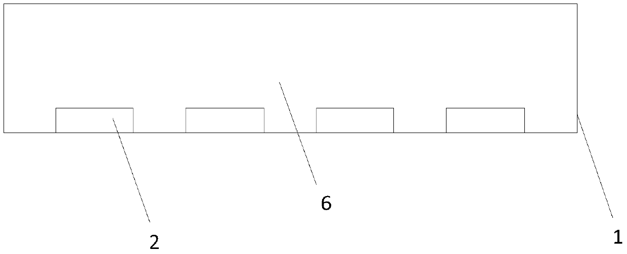
[0039] Step 101, the top chip 1 of the three-dimensional chip is provided with a top chip groove, and copper is deposited in the top chip groove and on the surface of the top chip 1, and the surface of the top chip 1 deposited with copper is chemically mechanically planarizing until the top silicon dioxide layer 6 is exposed, and the copper in the top chip trench is the top chip copper 2;

[0040] Step 102, depositing a silicon nitride layer 3 on the surface of the top chip 1 after chemical mechanical planarization;

[0041] Step 103, etching the silicon nitride layer 3 attached to the top chip copper 2 to form a gro...


PUM


Abstract

The invention relates to the field of semiconductor fabrication, in particular to a metal bonding method of a three-dimensional chip structure and a bonding structure. The method comprises that copper of a top chip is processed in a chemical machinery planarization mode, a silicon nitride layer is deposited on the surface after being processed in a chemical machinery planarization mode, the silicon nitride layer attached to the copper of the top chip is etched, a groove is formed, the bottom of the groove is the copper of the top chip, copper of a bottom chip is processed in a chemical machinery planarization mode, a bottom silica layer is etched, the copper is enabled to be protruded, activating treatment is carried out to the surface after etch of the copper of the bottom chip is achieved, the copper of the top chip and the copper of the bottom chip are aligned and bonded, and annealing treatment is carried out to the chips after being bonded. According to the metal bonding method of the three-dimensional chip structure and the bonding structure, silicon oxide and silicon nitride are used for being matched with metal and metal bonding, bonding quality is enabled to be better, a silicon nitride layer thin layer can prevent the metal from diffusing into around materials, and goals that a technology process is simplified, temperature needed by bonding is reduced, bonding reliability is improved, bonding efficiency is improved, and bonding cost is reduced can be achieved.

Description

technical field [0001] The invention relates to the field of semiconductor manufacturing, in particular to a metal bonding method and bonding structure of a three-dimensional chip structure. Background technique [0002] Integrating chips with different functions has become a trend in the development of integrated circuits. The large-scale integrated circuit manufacturing process is a planar manufacturing process that forms a large number of various types of semiconductor devices on the same substrate and interconnects them to have complete functions. Currently, most of the methods under development use TSV. After the chips are bonded, a deep through hole is made on the chip, and the metal parts in the two chips are connected by filling the metal material in the deep through hole. However, the current technology still suffers from the disadvantages of complexity, low reliability and high cost. Contents of the invention [0003] The technical problem to be solved by the ...

Claims


Application Information

Patent Timeline
Patent Type & Authority Applications(China)
IPC IPC(8): H01L21/768H01L23/522
Inventor 李平
Owner WUHAN XINXIN SEMICON MFG CO LTD
Why Eureka
Try Eureka