Nanometer dipole solar cell and preparation method thereof

A solar cell and dipole technology, applied in circuits, photovoltaic power generation, electrical components, etc., can solve problems such as increased equipment and maintenance costs, cross-contamination, and limiting the production speed of solar cells

Active Publication Date: 2013-05-15
INST OF ELECTRICAL ENG CHINESE ACAD OF SCI
View PDF5 Cites 4 Cited by
  • Summary
  • Abstract
  • Description
  • Claims
  • Application Information

AI Technical Summary

Problems solved by technology

This essential shortcoming of the prior art necessitates that each layer of material must be sequentially deposited separately during the production of solar cells
If different materials are deposited in a single vacuum chamber, cross-contamination can occur and limit the speed of solar cell production
If different targets are sputtered in different chambers, equipment and maintenance costs will increase

Method used


Image

  • Nanometer dipole solar cell and preparation method thereof
  • Nanometer dipole solar cell and preparation method thereof
  • Nanometer dipole solar cell and preparation method thereof

Examples


preparation example Construction

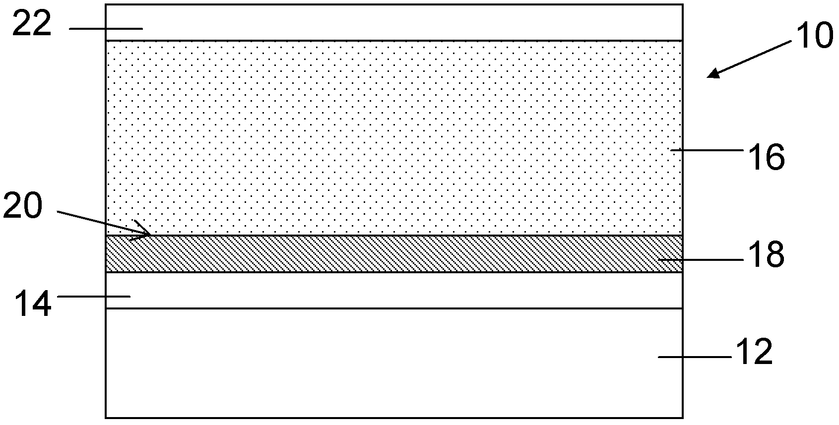
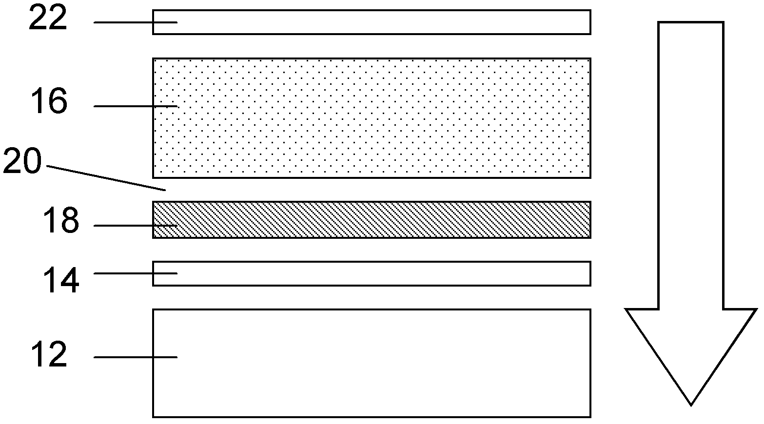
[0076] One of the preparation methods that the present invention prepares described nano-dipole solar cell comprises the following steps:

[0077] a) Clean the glass substrate covered with the first transparent conductive electrode layer, then sputter-deposit a mixed film of CdTe and CdS on the glass substrate, the thickness of the film is in the range of 0.2-20 μm, using The target material is CdS and CdTe mixed in a mass ratio of 1:30-1:2.5 and pressed;

[0078] b) Place the glass substrate deposited with CdTe and CdS mixed films on CdCl 2 Heat treatment in a mixed gas atmosphere with air for 5-120 minutes, and the heating temperature is 350-650 °C;

[0079] c) in CdCl 2 The second conductive electrode layer is deposited on the surface of the heat-treated film by sputtering to form the solar cell.

[0080] Error in implementing the steps described! Reference source not found. Simultaneously with b), applying a polarizing electric field on the first transparent conductiv...

Embodiment 1

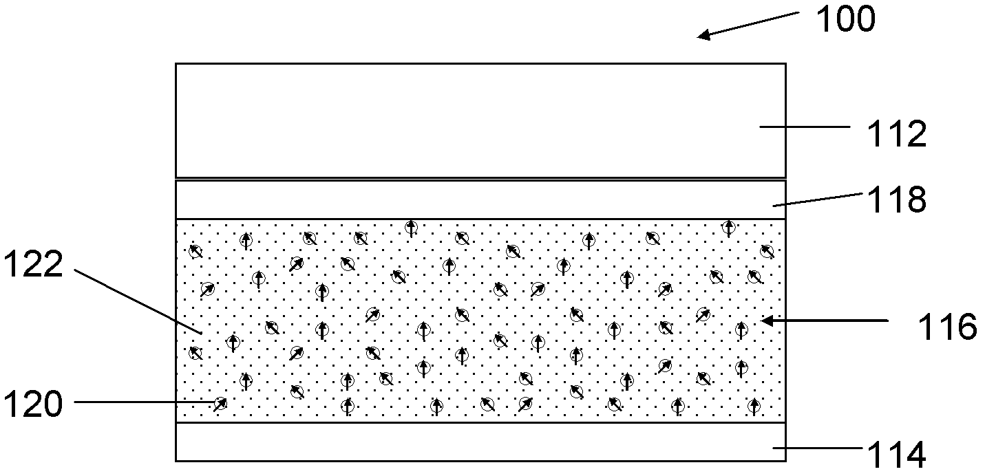
[0088] First install the 99.999% high-purity ZnO:Al target on the target position of the magnetron sputtering equipment; then send the cleaned glass substrate into the vacuum chamber of the thermal evaporation equipment and heat it to 200°C; Vacuum down to below 4×10 -4 Pa; fill the vacuum chamber with argon gas to 2Pa; turn on the RF sputtering power supply, and adjust the output power of the power supply to 2.5W / cm 2 , the distance between the target and the glass substrate is 10 cm; under this process condition, a 1.0 μm thick ZnO:Al transparent conductive film (TCO), that is, the first transparent conductive electrode layer, is deposited by sputtering.

[0089] Then mix CdS and CdTe according to the mass ratio of 1:30, at 6000N / cm 2The mixed target is pressed under a certain pressure, and the target made of the mixed target is installed on the target position of the magnetron sputtering equipment. Then the glass substrate deposited with the first transparent conductive e...

Embodiment 2

[0094] Install the 99.999% high-purity ZnO:Al target on the target position of the magnetron sputtering equipment; then send the cleaned glass substrate into the vacuum chamber of the thermal evaporation equipment and heat it to 200°C; pump the vacuum chamber Vacuum to below 4×10 -4 Pa; fill the vacuum chamber with argon gas to 2Pa; turn on the RF sputtering power supply, and adjust the output power of the power supply to 2.5W / cm 2 , the distance between the target and the glass substrate is 10 cm; under this process condition, a 1.0 μm thick ZnO:Al transparent conductive film (TCO), that is, the first transparent conductive electrode layer, is deposited by sputtering.

[0095] After mixing ZnTe and CdTe at a mass ratio of 1:30, at 10000N / cm 2 The mixed target is pressed under a certain pressure, and the target pressed from the mixed target is installed on the target position of the magnetron sputtering equipment. Then the TCO conductive glass substrate is sent into the vacu...


PUM

PropertyMeasurementUnit
Thicknessaaaaaaaaaa

Abstract

The invention provides a nanometer dipole solar cell and a preparation method thereof. A photovoltaic effect layer (116) is jointly formed by materials with photovoltaic effects and nanometer dipole particles embedded in the photovoltaic effect materials. The nanometer dipole particles have electric dipole moments or piezoelectric properties. The electric dipole moments of the nanometer dipole particles are polarized and at least parts of the electric dipole moments are arranged in the same direction. The direction of polarization of the nanometer dipole particles has weight in the direction perpendicular to a transparent electric conduction electrode layer or an electric conduction electrode layer, and the nanometer dipole particles provide a macroscopic electric field which is needed by separation of photoproduction charge. The photovoltaic effect layer can generate current and voltage when the photovoltaic effect layer receives electromagnetic wave radiation. Due to the fact that n-type mixed materials and p-type mixed materials are simultaneously deposited on a substrate, a needed solar cell is obtained.

Description

technical field [0001] The invention relates to a solar cell without plane junction electric field and a preparation method thereof. Background technique [0002] Solar cells typically use semiconductor materials with flat interfaces to harvest incident light energy and generate electricity. Semiconductor materials are generally divided into two categories: electron-rich materials, n-type semiconductor materials, and p-type semiconductors, which are rich in holes or electron-depleted states. When the solar cell is exposed to a light source, electrons in the n-type layer move and pass through the planar junction made of semiconductor materials to the p-type layer to generate current. The power generation capability of a solar cell is related to the surface area of ​​the p-n junction. A solar cell with a single p-n junction may have a larger surface area. Solar cells can use stacked structures to form multiple p-n junctions. In fact, a multi-junction solar cell is a stack ...

Claims


Application Information

Patent Timeline
IPC IPC(8): H01L31/0352H01L31/04H01L31/18G01R31/26H01L31/073H02S50/10
CPCY02E10/50Y02E10/543Y02P70/50
Inventor 刘向鑫
Owner INST OF ELECTRICAL ENG CHINESE ACAD OF SCI
Why Eureka
Try Eureka