Submicron surface plasmon polariton beam splitter based on composite cavity structure

A surface plasmon and beam splitter technology, applied in the field of nanophotonics, can solve the problems of low beam splitting ratio, unfavorable high integration, reduced device design and processing flexibility, etc., to improve integration and beam splitting performance Good, simple structure effect

Inactive Publication Date: 2013-05-22
PEKING UNIV
View PDF3 Cites 19 Cited by
  • Summary
  • Abstract
  • Description
  • Claims
  • Application Information

AI Technical Summary

Problems solved by technology

However, these additional grating structures greatly increase the size of the SPPs beam splitter, which is not conducive to high integration
Furthermore, the beam splitting of SPPs can also be realized by covering a layer of dielectric film with a finite thickness on the asymmetric nanometer single slit, but due to the increase of the dielectric film, the transmission distance of SPPs is shortened, and at the same time, the device design and processing costs are reduced. flexibility
Recently, it was proposed to use the different reflective properties of nanogrooves with different sizes to SPPs, that is, to prepare a pair of parallel nanogrooves with different widths to realize submicron beam splitters, but the beam splitting ratio is too low. Only beam splitting ratios of 3:1 and 1:2 are obtained at 650nm and 750nm respectively

Method used


Image

  • Submicron surface plasmon polariton beam splitter based on composite cavity structure
  • Submicron surface plasmon polariton beam splitter based on composite cavity structure
  • Submicron surface plasmon polariton beam splitter based on composite cavity structure

Examples


Embodiment Construction

[0019] The present invention will be further described through the embodiments below in conjunction with the accompanying drawings.

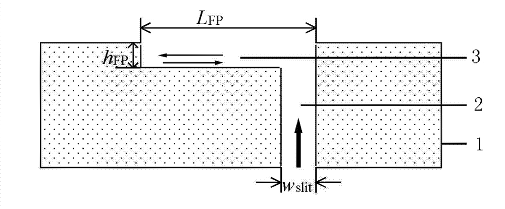
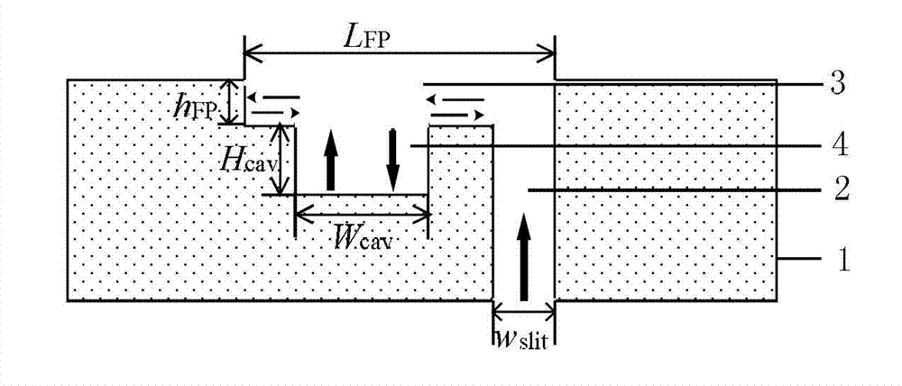
[0020] Such as figure 1 As shown, the nano-slit disposed on the metal film 1 and the nano-groove 3 on the left side of the nano-slit 2 form an asymmetric nano-single slit. An FP resonant cavity is formed between the left wall of the nanotrench and the right wall of the nanoslit. The metal film adopts a gold film, and the width of the nano-slit w slit =180nm, the length L of the FP cavity FP =790nm, the depth h of the nano-groove FP =120nm. Numerical simulations were carried out using the finite element method FEM. The dielectric constant of gold in the simulations as a function of wavelength was taken from the literature and developed by interpolation.

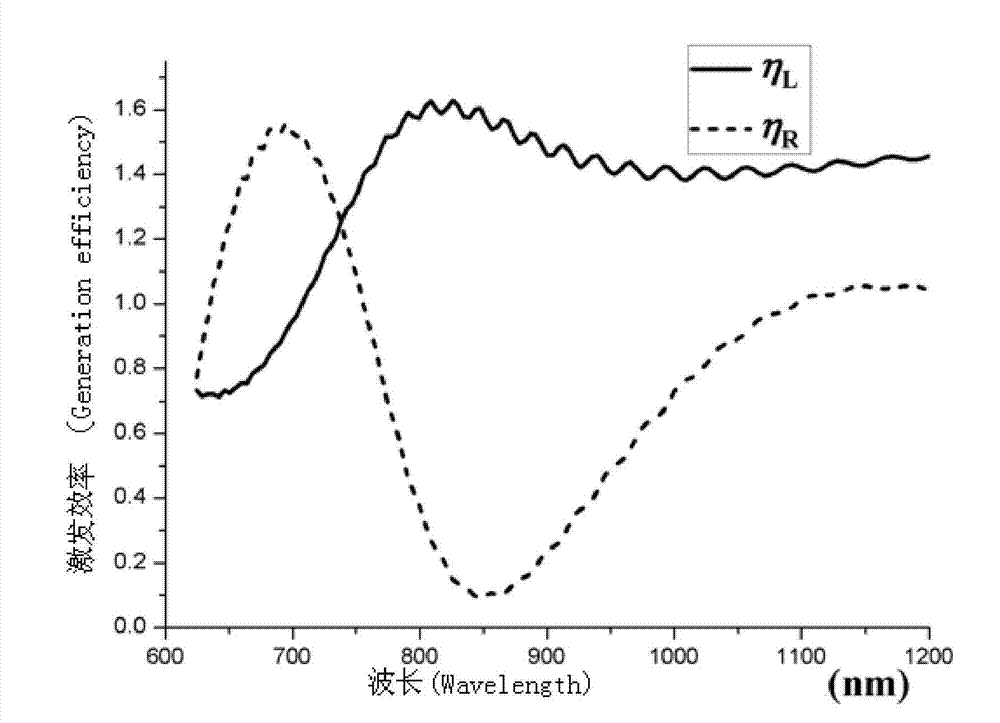
[0021] The simulation results are as figure 2 As shown in , it can be clearly seen that at λ=850nm, SPPs mainly propagate to the left. This is because the rightward propagating SPPs alo...


PUM

PropertyMeasurementUnit
thicknessaaaaaaaaaa

Abstract

The invention discloses a submicron surface plasmon polariton beam splitter based on a composite cavity structure. The surface plasmon polariton beam splitter comprises a metal thin film. A nanometer suture which can penetrate through an upper surface and a lower surface of the metal thin film are arranged on the metal thin film. A nanometer groove is formed on one side of the nanometer suture to form an asymmetric nanometer monolete suture. A metal-medium-metal metal injection molding (MIM) vertical cavity is integrated below the nanometer groove. On an operating wavelength of the beam splitter, a function point (FP) resonant cavity and the MIM vertical cavity are used for nearly manipulating surface plasmon polaritons (SPPs) independently, wherein the FP resonant cavity is formed in the upper half portion of the asymmetric nanometer monolete suture and the MIM vertical cavity is integrated in the FP resonant cavity. Therefore, the submicron surface plasmon polariton beam splitter based on the composite cavity structure has the advantages that SPPs beam splitting can be achieved. The greater advantage is that beam splitting wavelength can be allowed and convenient to adjust. Meanwhile, transverse size can not be increased, and the integrated height can be increased. In a high integration density plasmon polariton return circuit, the submicron surface plasmon polariton beam splitter based on the composite cavity structure has a potential application. The submicron surface plasmon polariton beam splitter based on the composite cavity structure is simple in structure, good in beam splitting performance, high in extinction ratio and capable of providing a design thought for other surface plasmon polariton function components.

Description

technical field [0001] The invention relates to the field of nanophotonics, in particular to a submicron surface plasmon beam splitter based on a composite cavity structure. Background technique [0002] Surface plasmon polaritons (Surface Plasmon Polariton) SPPs are currently a hot spot in nanophotonics research. The surface plasmon is a collective oscillation that exists at the interface between the metal and the medium coupled with the light wave and the free electrons in the metal. It is a special electromagnetic field in the interface bound mode. Its existence can be solved by solving the interface between the metal and the medium. It is obtained from Maxwell's equations under the boundary conditions. The biggest feature of SPPs is that they can localize the light field within the sub-wavelength size at the interface between the metal and the medium, breaking through the diffraction limit of traditional optics. At the same time, they also have a local field enhancement...

Claims


Application Information

Patent Timeline
Patent Type & Authority Applications(China)
IPC IPC(8): G02F1/01
Inventor 李智张翔廖慧敏陈建军龚旗煌
Owner PEKING UNIV
Why Eureka
Try Eureka