Non-refrigerating film infrared focal plane array detector structure and production method thereof

An infrared focal plane, array detector technology, applied in electrical radiation detectors, semiconductor devices, final product manufacturing, etc. The effect of thermal response characteristics, high filling rate, and good thermal isolation effect

Inactive Publication Date: 2013-05-22
SICHUAN UNIV
View PDF5 Cites 10 Cited by
  • Summary
  • Abstract
  • Description
  • Claims
  • Application Information

AI Technical Summary

Problems solved by technology

[0006] The purpose of the present invention is to overcome the deficiencies of the prior art, to provide a new type of uncooled thin-film infrared focal plane array detector structure and its preparation method, so as to meet the preparation requirements of large-scale arr

Method used


Image

  • Non-refrigerating film infrared focal plane array detector structure and production method thereof
  • Non-refrigerating film infrared focal plane array detector structure and production method thereof
  • Non-refrigerating film infrared focal plane array detector structure and production method thereof

Examples


Embodiment 1

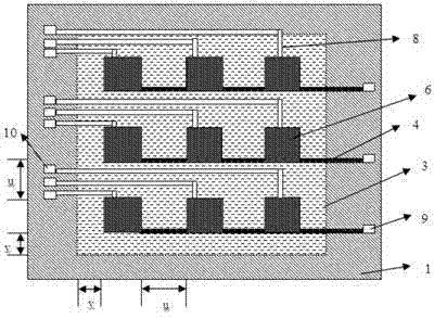
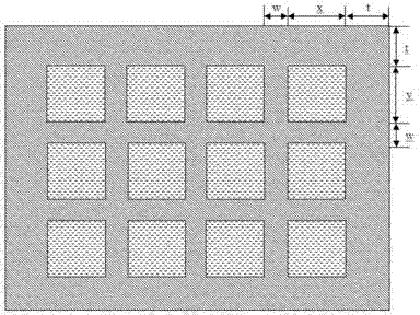
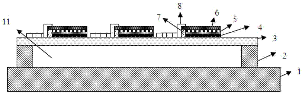
[0046] In this embodiment, the uncooled thin-film infrared focal plane array detector structure includes a first substrate 1 containing a readout circuit, a second substrate 2 containing a heat-isolated microbridge array and a sensitive element array, and the first substrate The sheet 1 and the second substrate 2 are bonded together by silicon-silicon bonding technology, and each thermally isolated microbridge unit in the thermally isolated microbridge array uses the etched second substrate 2 as a bridge pier to communicate with the The supporting layer 3 tightly bonded to the top surface of the bridge pier is the bridge deck, and the thickness of the air gap 11 of each heat-isolated micro-bridge unit is the same as the thickness of the second substrate, as figure 1 , figure 2 As shown; the first substrate 1 is a silicon substrate, the second substrate 2 is a double-polished silicon substrate, and the bridge deck (support layer 3) is SiO 2 Floor. The thermally isolated micr...

Embodiment 2

[0048] In this embodiment, the uncooled thin-film infrared focal plane array detector structure includes a first substrate 1 containing a readout circuit, a second substrate 2 containing a heat-isolated microbridge array and a sensitive element array, and the first substrate The sheet 1 and the second substrate 2 are bonded together by silicon-silicon bonding technology, and each thermally isolated microbridge unit in the thermally isolated microbridge array uses the etched second substrate 2 as a bridge pier to communicate with the The supporting layer 3 tightly bonded to the top surface of the pier is the bridge deck, and the thickness of the air gap 11 of each heat-isolated micro-bridge unit is the same as that of the second substrate; the first substrate 1 is a silicon substrate, and the second substrate 2 is Double polished silicon substrate, bridge deck (support layer 3) is SiO 2 / Si 3 N 4 composite layer. The thermally isolated microbridge array is composed of 8×8 id...

Embodiment 3

[0050] This embodiment is a method for preparing the uncooled thin-film infrared focal plane array detector structure described in Embodiment 1, and the steps are as follows:

[0051] (1) Preparation of the bonding surface pattern of the first substrate

[0052] A silicon wafer is used as the first substrate 1, and a titanium film with a thickness of 30 nm is deposited on the surface of the first substrate 1 containing the readout circuit, and a gold film with a thickness of 120 nm is deposited on the surface of the titanium film, and then according to the design Photolithographic graphics of the electrode and bonding surface pattern to realize the patterning of the bonding surface;

[0053] (2) Preparation of support layer

[0054] A double-polished silicon wafer is used as the second substrate 2, and both sides of the second substrate are thermally oxidized to form a layer of 600nm thick and dense SiO on both sides. 2 layer; select one side as the support layer 3, which is...


PUM

PropertyMeasurementUnit
Thicknessaaaaaaaaaa
Widthaaaaaaaaaa
Thicknessaaaaaaaaaa

Abstract

A non-refrigerating film infrared focal plane array detector structure comprises a first substrate provided with reading circuits, and a second substrate provided with thermal isolation microbridge arrays and sensitive element arrays. The first substrate and the second substrate are integrally bonded. The etched second substrate serves as a pier for each thermal isolation microbridge unit in the thermal isolation microbridge arrays, and a support layer tightly attached to the top of the pier serves as a deck. The deck of each thermal isolation microbridge unit is provided with one sensitive element array. Each sensitive element array is electrically connected with the corresponding reading circuit of the first substrate through a lead electrode. A production method of the non-refrigerating film infrared focal plane array detector structure includes: preparing a pattern on a bonding surface of the first substrate, preparing the support layer, preparing the sensitive element arrays, protecting the front side of the second substrate, preparing the thermal isolation microbridge arrays, bonding the first substrate and the second substrate, removing a front protective layer of the second substrate, and connecting electrodes of the sensitive element electrode reading circuits.

Description

technical field [0001] The invention belongs to the field of microelectronic devices, in particular to an uncooled thin-film infrared focal plane array detector structure and a preparation method thereof Background technique [0002] The uncooled thin-film infrared focal plane array detector is a thermal radiation detection device based on the principle of thermal effect, and its core part is a sensitive element array with thermal sensing capability. The thermal detection capability of the sensor can be effectively improved by adding a thermally isolated microbridge. In order to improve the performance of the sensor and the entire detector, people continue to improve the structure of the thermally isolated microbridge. The thin-film uncooled infrared focal plane array detector structures reported so far that can be integrated with the readout circuit can be divided into two categories: one is the sacrificial layer technology based on surface micromachining technology, that i...

Claims


Application Information

Patent Timeline
IPC IPC(8): H01L27/144G01J5/20H01L31/18
CPCY02P70/521Y02P70/50
Inventor 余萍陈潇洋王晓峰杨春丽胡旭朱建国张小山徐尊平
Owner SICHUAN UNIV
Why Eureka
Try Eureka