Metal oxide semiconductor field effect transistor (MOSFET) with lifted silicide source drain contact and manufacture method thereof

A manufacturing method and a technology of source-drain contact, applied in semiconductor/solid-state device manufacturing, semiconductor devices, electrical components, etc., can solve the problems of reducing the total resistance of the device, failing to effectively reduce the interconnection resistance, and affecting the electrical performance of semiconductor devices. The effect of reducing interconnection resistance, reducing dosage, and improving electrical performance

Inactive Publication Date: 2013-06-05
INST OF MICROELECTRONICS CHINESE ACAD OF SCI
View PDF5 Cites 4 Cited by
  • Summary
  • Abstract
  • Description
  • Claims
  • Application Information

AI Technical Summary

Problems solved by technology

[0006] However, since the top of the first metal contact 6A is substantially flush with the top of the gate 3, that is, the metal contact of W material still has a considerable thickness, so its interconnection resistance is still considerable, which cannot effectively and appreciably reduce the total device size. resistance

Method used


Image

  • Metal oxide semiconductor field effect transistor (MOSFET) with lifted silicide source drain contact and manufacture method thereof
  • Metal oxide semiconductor field effect transistor (MOSFET) with lifted silicide source drain contact and manufacture method thereof
  • Metal oxide semiconductor field effect transistor (MOSFET) with lifted silicide source drain contact and manufacture method thereof

Examples


Example Embodiment

[0029] The features and technical effects of the technical solutions of the present invention are described in detail below with reference to the accompanying drawings and schematic embodiments, and a semiconductor device and a manufacturing method thereof that can effectively reduce interconnect resistance are disclosed. It should be noted that similar reference numerals denote similar structures, and the terms "first", "second", "upper", "lower", etc. used in this application may be used to modify various device structures or fabrication processes . These modifications do not imply a spatial, sequential, or hierarchical relationship of the modified device structures or fabrication processes unless otherwise specified.

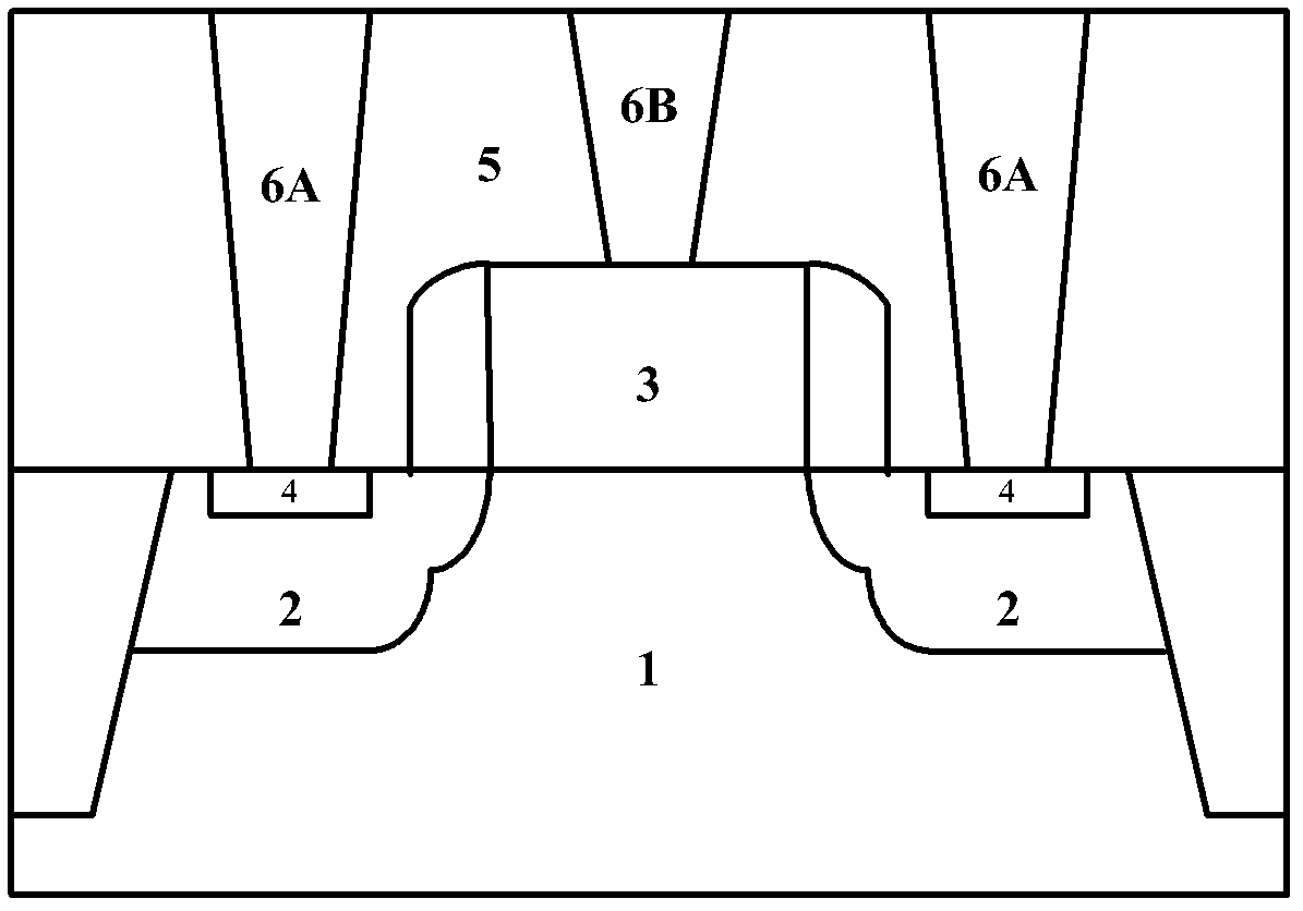
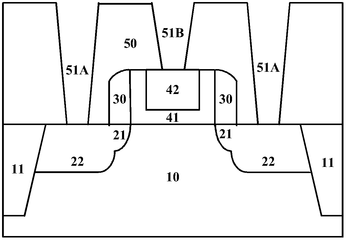
[0030] First, refer to image 3 , forming contact holes in the base structure.

[0031] Specifically, the substrate 10 is provided first. The substrate 10 may be bulk silicon, silicon-on-insulator (SOI), or a compound semiconductor substrate such as SiGe, ...


PUM


Abstract

The invention discloses a semi-conductor device which comprises a substrate, a source drain region in the substrate, a grid stacking structure on the substrate, a grid lateral wall, first metal silicide in the source drain region, contact plugs arranged above the source drain region and the grid stacking structure respectively and an interlayer dielectric layer. The semi-conductor device is characterized in that second metal silicide is arranged on the first metal silicide and the grid stacking structure, and the contact plugs are contacted with the second metal silicide. By means of the semi-conductor device, by lifting the first metal silicide, the first metal silicide is higher than the surface of the source drain region, and use amount of W in a contact hole is reduced. Interconnection resistance is greatly reduced, Cu diffusion can be effectively resisted, and the electrical performance of the device is effectively improved on the whole.

Description

technical field [0001] The invention relates to a semiconductor device and a manufacturing method thereof, in particular to a MOSFET with raised silicide source-drain contacts and a manufacturing method thereof. Background technique [0002] Such as figure 1 As shown, it is a schematic cross-sectional view of a traditional metal-oxide-semiconductor field effect transistor (MOSFET), which at least includes a silicon substrate 1, a source and drain region 2, a gate 3, a metal silicide 4, an interlayer dielectric layer (ILD ) 5 (usually phosphosilicate glass PSG), metal contact 6. Wherein, the metal silicide 4 is formed in the source and drain region 2 to reduce the contact resistance, but since the process of forming the metal silicide 4 is through metal (usually including Ni, Pt, Co, etc.) reacting with silicon in the source and drain region 2 and It is formed by partially consuming silicon, so usually the top surface of the metal silicide 4 basically does not exceed the to...

Claims


Application Information

Patent Timeline
IPC IPC(8): H01L29/417H01L29/78H01L21/28H01L21/336
Inventor 罗军赵超钟汇才李俊峰陈大鹏
Owner INST OF MICROELECTRONICS CHINESE ACAD OF SCI
Why Eureka
Try Eureka