Method for preparing low-density and long-wavelength indium arsenide/gallium arsenide (InAs/GaAs) quantum dots

A long-wavelength, low-density technology, applied in the field of molecular beam epitaxy, can solve the problems of limited extraction efficiency, small quantum dot size, lack of space constraints for carriers, etc., achieving the effect of easy control of density and uniform size

A long-wavelength, low-density technology, applied in the field of molecular beam epitaxy, can solve the problems of limited extraction efficiency, small quantum dot size, lack of space constraints for carriers, etc., achieving the effect of easy control of density and uniform size

CN103137789AInactive Publication Date: 2013-06-05INST OF SEMICONDUCTORS - CHINESE ACAD OF SCI

Image

  • Method for preparing low-density and long-wavelength indium arsenide/gallium arsenide (InAs/GaAs) quantum dots
  • Method for preparing low-density and long-wavelength indium arsenide/gallium arsenide (InAs/GaAs) quantum dots
  • Method for preparing low-density and long-wavelength indium arsenide/gallium arsenide (InAs/GaAs) quantum dots

Examples


Embodiment Construction

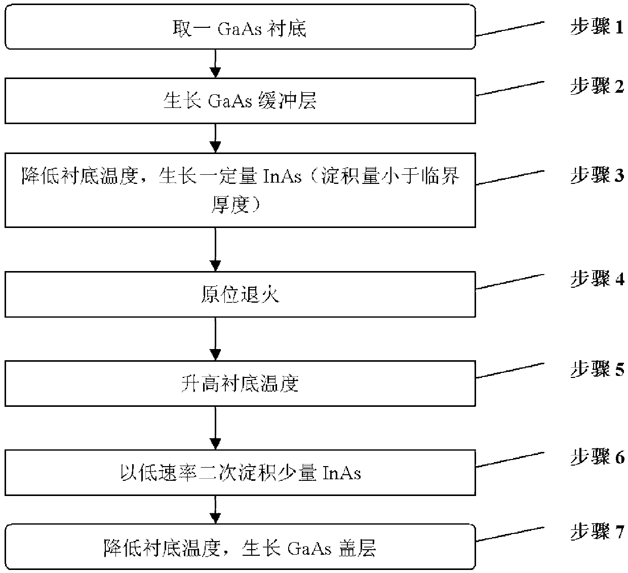
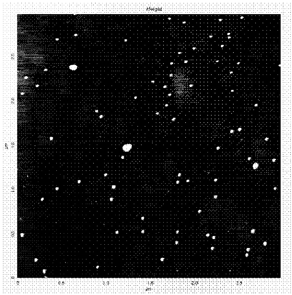
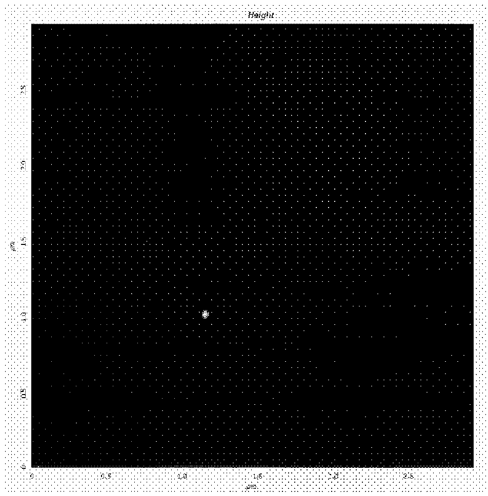
[0024] see figure 1 As shown, the present invention provides a method for preparing low-density, long-wavelength InAs / GaAs quantum dots, comprising the steps of:

[0025] Step 1: Take a liner, put the substrate into the molecular beam epitaxy equipment after pretreatment such as degassing, and the substrate material is GaAs;

[0026] Step 2: Deposit a growth buffer layer on the substrate; grow a GaAs buffer layer on the GaAs substrate and other epitaxial layers that match the substrate lattice; in this step, the substrate temperature is 580°C, and the thickness of the GaAs buffer layer is Unlimited, unlimited growth rate.

[0027] Step 3: Deposit and grow an InAs layer on the buffer layer, suspend the deposition and growth when the critical thickness is not reached, the temperature of the deposition and growth InAs layer is 470°C-490°C, the growth rate is 0.01-0.1ML / s, pause The deposited and grown InAs layer is 0.05-0.5ML less than the critical thickness; the substrate temp...


PUM


Abstract

The invention provides a method for preparing low-density and long-wavelength indium arsenide / gallium arsenide (InAs / GaAs) quantum dots. The method includes a first step of picking up a substrate, a second step of depositing and growing a buffer layer on the substrate, a third step of depositing and growing an InAs layer on the buffer layer, suspending deposition and growth when the InAs layer does not reach the critical thickness, a fourth step of annealing the substrate with the growing InAs layer, a fifth step of rising temperature of the substrate after annealing, a sixth step of growing the InAs layer through secondary deposition, a seventh step of depositing and growing a GaAs cover layer on the InAs layer which grows through the secondary deposition, and obtaining the low-density and long-wavelength InAs / GaAs quantum dot structure. The method can be used for preparing the low-density InAs / GaAs quantum dots with room temperature luminous long-wavelength longer than 1.3 micrometers.

Description

technical field [0001] The invention relates to the field of semiconductor materials and optoelectronic technology, in particular to a growth method of low-density, large-size, and long-wavelength quantum dots, in particular to a molecular beam epitaxy method for growing low-density, long-wavelength InAs quantum dots on a GaAs substrate. Background technique [0002] In recent years, with the development of high-quality self-organized quantum dot technology, the research of semiconductor quantum dots in quantum optics and quantum communication has attracted more and more people's interest. These quantum dots not only finally realize the three-dimensional confinement of the carriers, resulting in the carriers having discrete energy levels due to the quantization of energy in three dimensions, showing some energy level characteristics similar to the shell structure of atoms, but also Also native to solid systems, they can be tuned to produce photons with nonclassical statistic...

Claims


Application Information

Patent Timeline
05 Jun 2013
Publication
CN103137789A
IPC
H01L31/18
CPC
Y02P70/521; Y02P70/50
Inventors
张世著; 叶小玲