
MEMS (micro-electromechanical system) chip and wafer level encapsulation cover plate grounding method of MEMS chip

A technology of wafer-level packaging and grounding method, which is applied in the fields of crafts, decorative arts, and measuring devices used to produce decorative surface effects, and can solve problems such as flushing out lines, affecting yields, and long grounding wires, etc., to achieve packaged finished products High efficiency, firm adhesion, not easy to fall off

Active Publication Date: 2013-06-12
ANHUI BEIFANG XINDONG LIANKE MICROSYST TECH
View PDF6 Cites 10 Cited by
  • Summary
  • Abstract
  • Description
  • Claims
  • Application Information

AI Technical Summary

Problems solved by technology

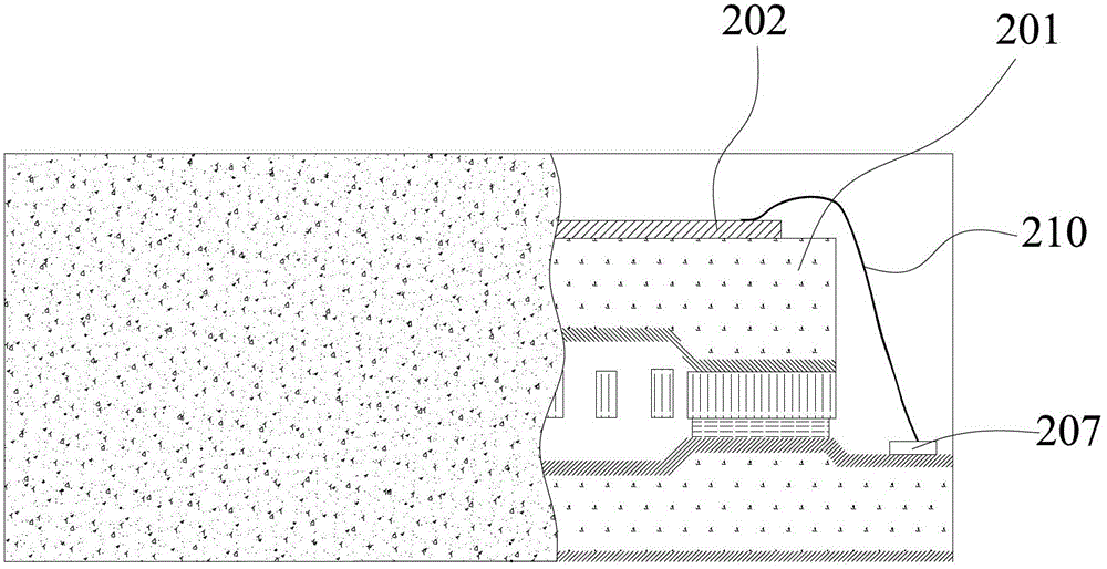
This method is to ground the cover plate of the MEMS chip through wire bonding. The upward pulling arc part of the grounding wire 210 has a certain height, and the thickness of the package cannot be reduced. In those application fields that are sensitive to the thickness of electronic components, such as mobile phones, etc. In electronic devices, the use is restricted
In addition, the height difference between the metal wire 202 of the MEMS chip and the pad 207 is relatively large, and the ground wire 210 is relatively long. In the subsequent pressurized injection molding process, the force is relatively large, and it is easy to be washed off the wire, which affects the yield.

Method used


Image

  • MEMS (micro-electromechanical system) chip and wafer level encapsulation cover plate grounding method of MEMS chip
  • MEMS (micro-electromechanical system) chip and wafer level encapsulation cover plate grounding method of MEMS chip
  • MEMS (micro-electromechanical system) chip and wafer level encapsulation cover plate grounding method of MEMS chip

Examples


Embodiment Construction

[0023] The present invention will be further described below in conjunction with drawings and embodiments.

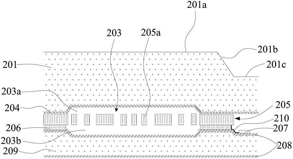
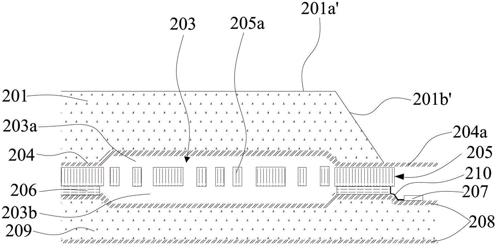
[0024] Such as Figure 6 and Figure 7 As shown, the MEMS chip is composed of a cover plate 201, a MEMS structure layer 205 and a bottom plate 209. The bottom of the cover plate 201 has an upper cavity 203a with an opening downward, and the bottom plate 209 has an upper cavity 203b with an upward opening. The upper cavity 203a Form a sealed cavity 203 with the lower cavity 203b, the movable part 205a of the MEMS structure layer 205 is located in the sealed cavity 203, and can move freely in the sealed cavity 203, there is a cover plate insulation between the cover plate 201 and the MEMS structure layer 205 The layer 204 is isolated, and there are metal wires 202 on the surface 201a' of the cover plate and the inclined side surface 201b' of the cover plate, wherein the metal wire 202 on the inclined side surface of the cover plate electrically connects the cover plate 2...


PUM


Abstract

The invention relates to an MEMS (micro-electromechanical system) chip and a wafer level encapsulation cover plate grounding method of the MEMS chip. The MEMS chip consists of a cover plate, a cover plate insulating layer, an MEMS structure layer, a conducting welding flux layer, a bottom plate insulating layer and a bottom plate, wherein a metal conducting wire is arranged on the cover plate, the cover plate is electrically connected with the MEMS structure layer through the metal conducting wire, a pressure welding block is arranged on the bottom plate insulating layer, and the pressure welding block is electrically connected with the MEMS structure layer through a grounding conducting wire. In the subsequent encapsulation process, the cover plate grounding goal can be realized only when the pressure welding block is connected onto an encapsulation carrier. The cover plate grounding method is characterized in that firstly, the maskless lithography is carried out, the MEMS structure layer is exposed, then, the metal conducting wire is sputtered on the cover plate and the MEMS structure layer, and the cover plate and the MEMS structure layer are electrically connected through the metal conducting wire. Therefore, the cover plate and the pressure welding block realize the electric connection through the metal conducting wire and the grounding conducting wire, and the goal of the cover plate grounding is reached. The method provided by the invention has the advantages that the total thickness of the chip is reduced, the miniaturization encapsulation is convenient, the metal conducting wire is formed through deposition by a sputtering method, the cost is low, and the wire loosing cannot easily occur.

Description

technical field [0001] The invention belongs to the field of chip packaging, and in particular relates to a MEMS chip, and also relates to a grounding method for a cover plate of the MEMS chip wafer-level packaging. Background technique [0002] Electronic packaging is to electrically connect one or more electronic chips to each other, and then encapsulate them in a protective structure, the purpose of which is to provide electrical connection, mechanical protection or chemical corrosion protection for electronic chips. However, for some electronic products, the surface of the chip cannot be in contact with the packaging material, especially some micro sensors, such as MEMS devices, surface acoustic wave / bulk acoustic wave filters, oscillators, etc., need to be sealed with ceramic shells, metal shells or plastic shells, etc. Hermetic packaging, but these packaging methods are costly and bulky, making them unsuitable for consumer electronics. The development trend of packagi...

Claims


Application Information

Patent Timeline
IPC IPC(8): B81B7/00B81C1/00
Inventor 华亚平
Owner ANHUI BEIFANG XINDONG LIANKE MICROSYST TECH
Learn More