Production process for screen printed circuit board

A technology of screen printing and production process, applied in printed circuit, printed circuit manufacturing, printed circuit secondary treatment, etc., can solve the problems of low production efficiency, production cost can not be further reduced, silver paste blocking, etc.

Inactive Publication Date: 2013-06-12
杭州新三联电子有限公司
View PDF2 Cites 8 Cited by
  • Summary
  • Abstract
  • Description
  • Claims
  • Application Information

AI Technical Summary

Problems solved by technology

But now, for the circuit boards of this kind of products, many circuit board manufacturers use the film exposure method and the wet film method for the graphics and solder mask production of the products, so that the production cost cannot be further reduced, and the production efficiency is relatively low, and It will also cause the silver paste in the hole of the silver paste through hole / copper paste through hole to be blocked by the solder resist ink that removes the film, causing the product to have a hidden danger of non-conduction on both sides of the line; for silver cross-line products, then It will cause a great hidden danger to the bonding force of silver paste and copper foil

Method used


Image

  • Production process for screen printed circuit board
  • Production process for screen printed circuit board
  • Production process for screen printed circuit board

Examples


Embodiment 1

[0020] Embodiment 1: A production process of screen printed circuit boards, comprising the following steps: substrate cutting - edge grinding - NC drilling - deburring - graphic pretreatment - surface B screen printing graphic photocurable resist ink - UV light Curing—A side screen printing graphic photocurable resist ink—UV curing—etching, film removal—pretreatment for solder mask printing—A side screen printing photocurable solder resist ink—UV curing—B side screen printing photocurable resist Soldering ink—UV curing—silver paste / copper paste through hole printing pretreatment—silver paste / copper paste through hole screen printing—silver paste / copper paste hot air pre-drying, drying—preprinting treatment—A\B side silver paste / Copper paste protective layer printing and UV curing—A\S surface text printing machine curing—subsequent production process.

Embodiment 2

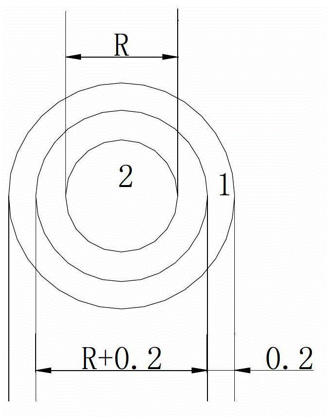
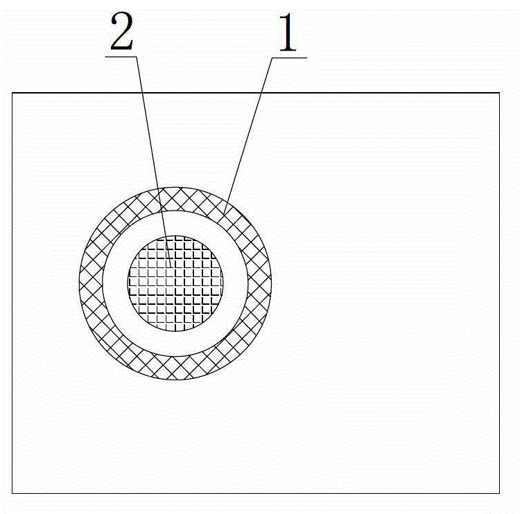
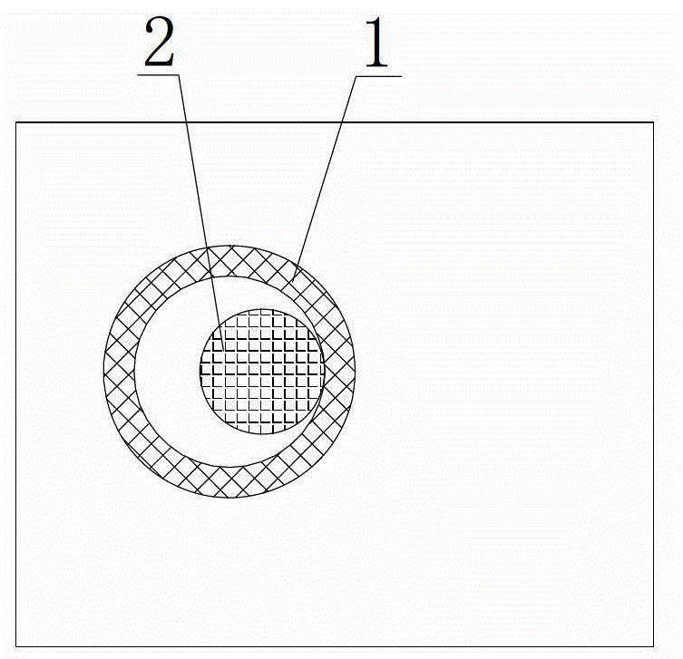
[0021] Embodiment 2: refer to Figure 1~4 . When the substrate is subjected to the NC drilling process step, the printing positioning hole and the punching positioning hole are drilled at one time as the reference hole 2 for graphic printing matching, and the diameter of the reference hole 2 is R; Make a ring pattern matching the reference hole 2 on the photo of the net making, that is, the pattern line 1, the ring width is 0.2mm, and the diameter of the inner ring is the reference hole diameter R+0.2mm, and the screen printing pattern light on the B side is printed by screen printing. Curing the anti-corrosion ink, checking the matching and coincidence degree of the graphic circuit 1 and the reference hole 2, that is, judging whether the matching accuracy of the graphic circuit 1 and the reference hole 2 meets the requirements with the naked eye; after printing and curing the graphic on the B side, carry out the graphic printing on the A side , the same as the above printing...


PUM


Abstract

The invention relates to a production process for a screen printed circuit board. The production process for the screen printed circuit board comprises the following steps of: performing substrate cutting, edging, performing numerical control (NC) drilling, deburring, performing graphic preprocessing, printing graphic photocurable anti-corrosion ink on a B-side screen, performing ultraviolet (UV) photocuring, printing the graphic photocurable anti-corrosion ink on an A-side screen, performing UV curing, etching and decoating, performing treatment before solder resist printing, printing photocurable solder resist ink on the A-side screen, performing the UV curing, printing the photocurable solder resist ink on the B-side screen, performing the UV curing, performing treatment before silver paste / copper paste through hole printing, performing silver paste / copper paste through hole screen printing, performing silver paste / copper paste hot air predrying and drying, performing treatment before printing, performing A / B-side silver paste / copper paste protective layer printing and the UV curing, curing characters on A / S sides by a printing machine, and performing follow-up production processes.

Description

technical field [0001] The invention relates to a production process of a screen printed circuit board. Background technique [0002] Screen printing is a traditional and widely used production process in the circuit board industry. The screen printing process has the advantages of low production cost, high production efficiency, and relative environmental protection. However, due to the problems of relatively poor printing accuracy and printing positioning deviation in the screen printing process, the screen printing process is generally only suitable for the production of single-sided or pseudo-double-sided products with simple lines and low graphics accuracy requirements. The field is extremely limited. [0003] From the perspective of the development process and trend of the circuit board industry, in the application of circuit board products, on the one hand, the accuracy of circuit boards is required to be higher and higher, and on the other hand, it is hoped to reduc...

Claims


Application Information

Patent Timeline
Patent Type & Authority Applications(China)
IPC IPC(8): H05K3/00H05K3/06H05K3/28H05K3/42
Inventor 俞军荣吴为王建峰姚丽萍陈怀谷郦诚吴兵彭静
Owner 杭州新三联电子有限公司
Why Eureka
Try Eureka