Method for producing solar cell and film-producing device

A technology of solar cells and manufacturing methods, applied to circuits, photovoltaic power generation, electrical components, etc., to achieve the effect of improving electrical characteristics

CN103155163AActive Publication Date: 2013-06-12SHIN ETSU CHEM IND CO LTD
4 Cites 4 Cited by

Patent Information

Authority / Receiving Office
CN · China
Patent Type
Applications(China)
Current Assignee / Owner
Publication Date
2013-06-12

Smart Images

  • Figure 1
    Figure 1
  • Figure 2
    Figure 2
  • Figure 3
    Figure 3
Patent Text Reader

Abstract

Disclosed is a method that is for producing a solar cell and that is characterized by performing an annealing step on a semiconductor substrate before an electrode-forming step. By means of performing annealing in the above manner, it is possible to improve the electrical characteristics of the solar cell without negatively impacting reliability or outward appearance. As a result, the method can be widely used in methods for producing solar cells having high reliability and electrical characteristics.
Need to check novelty before this filing date? Find Prior Art

Description

technical field

[0001] The present invention relates to a manufacturing method and a film forming apparatus of a solar cell. Background technique

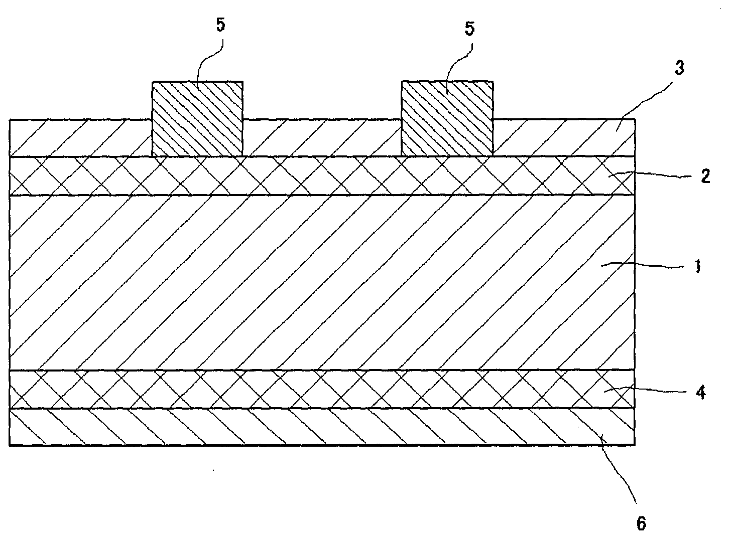
[0002] Typically, solar cells have figure 1 structure shown in . exist figure 1 Among them, 1 is a plate-shaped p-type semiconductor substrate with a size of 100-150 mm square and a thickness of 0.1-0.3 mm, made of polycrystalline silicon or single crystal silicon, and doped with p-type impurities such as boron. The substrate is doped with n-type impurities such as phosphorus to form an n-type diffusion layer 2, and an anti-reflection film 3 such as SiN (silicon nitride) is provided. After printing a conductive aluminum paste on the back surface by a screen printing method, drying, The back surface electrode 6 and the BSF (Back Surface Field) layer 4 are simultaneously formed by firing, and the collector electrode 5 is formed by printing a conductive silver paste on the front surface, followed by drying and firing. Thus, a so...

Examples

Embodiment

[0055] Hereinafter, although an Example and a comparative example are shown and this invention is concretely demonstrated, this invention is not limited to the following Example.

[0056] [Example, comparative example]

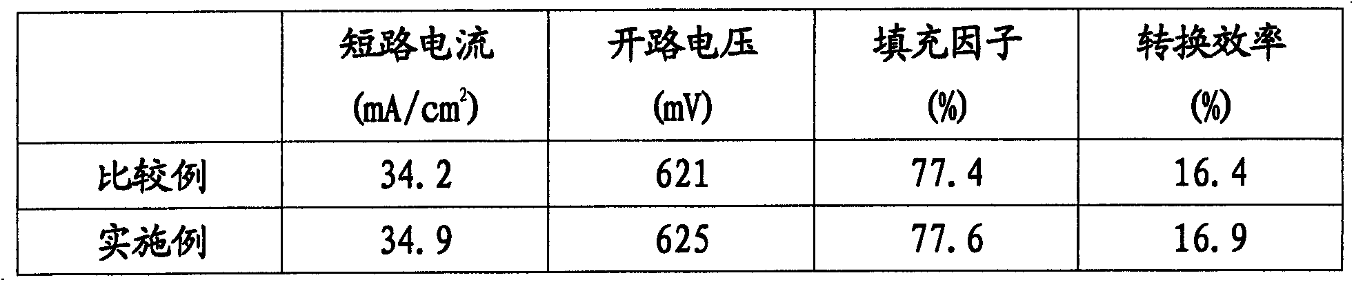
[0057] The outer diameter of a p-type silicon substrate made of p-type single crystal silicon with a resistivity of about 1 Ω·cm, which is doped with boron and sliced ​​into a thickness of 0.2 mm, is made into a square plate shape with a side of 15 cm. . Then, the p-type silicon substrate was immersed in a fluoronitric acid solution for 15 seconds to perform damage etching, and further, by chemical etching in a 70° C. solution containing 2% by mass of KOH and 2% by mass of IPA for 5 minutes, then using Wash and dry to form a textured structure on the surface of the p-type silicon substrate. Next, for the p-type silicon substrate, in POCl 3 An n layer was formed on a p-type silicon substrate by a thermal diffusion method in a gas atmosphere at a temperature ...