Method for preparing patterning silicon nanometer well array

A silicon nano-patterning technology, applied in gaseous chemical plating, manufacturing microstructure devices, and processes for producing decorative surface effects, etc. It can solve the period and diameter, and the depth can be precisely adjusted at the same time, and nano-well structures cannot be realized. problem, to achieve the effect of fast processing speed, low cost and simple system

Inactive Publication Date: 2013-06-19
UNIV OF SCI & TECH BEIJING
View PDF7 Cites 11 Cited by
  • Summary
  • Abstract
  • Description
  • Claims
  • Application Information

AI Technical Summary

Problems solved by technology

[0006] In the present invention, the combination of three-beam laser interference lithography technology and metal catalytic etching technology is used. At present, there is

Method used


Image

  • Method for preparing patterning silicon nanometer well array
  • Method for preparing patterning silicon nanometer well array
  • Method for preparing patterning silicon nanometer well array

Examples


Embodiment Construction

[0024] The technical solution of this scheme is described below in conjunction with examples, and the described examples cannot cover all scopes of the invention. Based on the examples in the present invention, all other examples obtained by those skilled in the art without making creative efforts belong to the protection scope of the present invention.

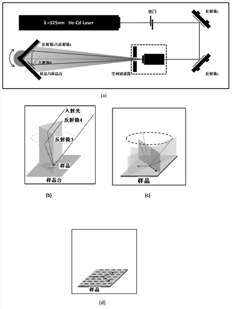
[0025] (1) Three-beam laser interference system: such as figure 1As shown in (a), a beam of 325nm laser is emitted by the He-Cd laser, passes through the electronic shutter, mirrors 1 and 2, and the spatial filter expands the beam to form a circular spot and irradiates the sample stage; figure 1 As shown in (b), the two mirrors (mirror 3 and mirror 4) form an angle of 120° to each other, and are perpendicular to the plane where the sample is placed, and the intersection point of the three surfaces is located in the center of the spot, so that the circular spot is divided into three equal parts. Among them, two beams of lig...


PUM

PropertyMeasurementUnit
Thicknessaaaaaaaaaa
Apertureaaaaaaaaaa

Abstract

The invention provides a method for preparing a patterned silicon nano well array. The method is realized by combination of a three-light-beam laser interference photolithography and a metal catalysis corrosion technology. Through adoption of the method provided by the invention, the patterned silicon nanometer well array which is arrayed regularly can be prepared in large area, and the precise regulation of array structure period, nano well diameter and nano well depth can be realized. Through changing the three-light-beam exposure conditions, phtoresist template with different sizes can be obtained, and the structure unit period and structure unit size of the nano well array can be regulated and controlled; and through control of etching time, the depth of the nano well is regulated. Besides the patterned silicon nano well array can be prepared in large area and nano well array is regulated, the patterned silicon nano well array has the characteristics of simple system, low cost, rapid processing speed and high yield and is suitable for batch production, and the finished product can realize different effects through simple processing.

Description

technical field [0001] The invention belongs to the field of patterned preparation of nanometer materials, and in particular relates to the preparation of a patterned silicon nanowell array by a template method. [0002] Background technique [0003] Nanowell arrays on silicon substrates have become the basis of new functional nanomaterials due to their large specific surface area and excellent ability to absorb waves. Silicon-based nanostructured materials have important applications in many fields ([1] Huang, Z.; Geyer, N.; Werner, P.; Boor, J; Gosele, U. Adv. Mater. 2011, 23, 285-308). For example, photoelectric sensors ([2] Tian, ​​B.; Zheng, X.; Kempa, T.J.; Fang, Y.; Yu, N.; Yu, G.; Huang, J.; Lieber, C.M. Nature 2007, 499, 885-890), light-absorbing materials to make energy conversion devices ([3] Peng, K.Q.; Xu, Y.; Wu, Y.; Yan, Y.J.; Lee, S.T.; Zhu, J. small 2005, 1, 1062-1067,[4] Hwang, Y.J.; Boukai, A.; Yang, P.D. Nano Lett. 2009, 9(1), 410-415), templates ...

Claims


Application Information

Patent Timeline
IPC IPC(8): B81C1/00
Inventor 张跃冯亚瀛陈翔李峻野方思萦徐佳亮孙国帅冯韵迪闫小琴
Owner UNIV OF SCI & TECH BEIJING
Why Eureka
Try Eureka