Method for manufacturing LED package
A technology of LED packaging and manufacturing method, applied in electrical components, electric solid devices, circuits, etc., can solve the problems of shortened life of LED packaging, poor thermal conductivity of insulating layer, yellowing radiation efficiency, etc., to improve light irradiation efficiency and improve heat dissipation. Efficiency, the effect of simplifying the manufacturing process
- Summary
- Abstract
- Description
- Claims
- Application Information
AI Technical Summary
Problems solved by technology
Method used
Image

Examples
Embodiment Construction
[0027] The above-mentioned object, technical configuration, functional effect, etc. of the manufacturing method of the LED package according to the present invention will be more clearly understood by referring to the following detailed description with reference to the accompanying drawings showing preferred embodiments of the present invention.
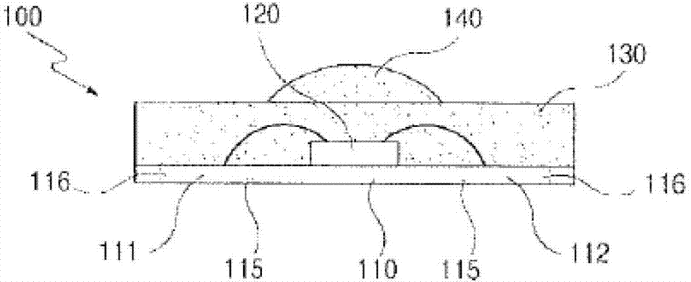
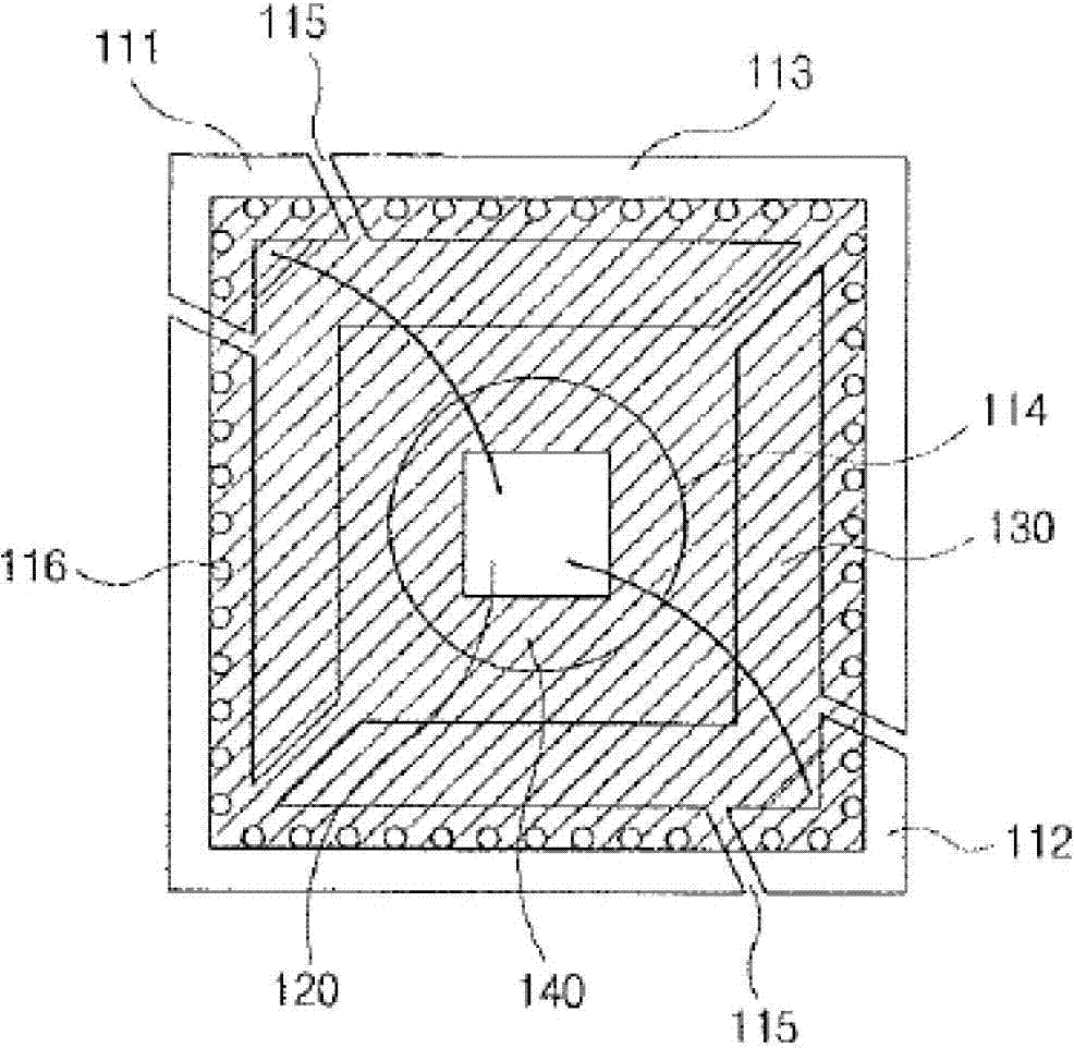
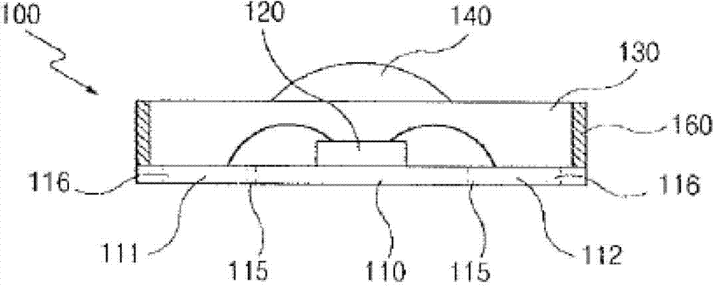
[0028] figure 1 is a cross-sectional view showing an LED package according to the present invention, figure 2 is a plan view showing the LED package according to the present invention.
[0029] As shown in the figure, the LED package 100 according to the present invention may include: a metal substrate 110, which has an anode terminal 111 and a cathode terminal 112; an LED chip 120, which is mounted on the metal substrate 110; a plastic package 130, which is packaged on the metal substrate 110 ; and the lens part 140 , which is integrally formed with the plastic sealing part 130 .
[0030] The metal substrate 110 may be composed ...
PUM
 Abstract
Description
Claims
Application Information
 - R&D
- Intellectual Property
- Life Sciences
- Materials
- Tech Scout
- Unparalleled Data Quality
- Higher Quality Content
- 60% Fewer Hallucinations
Browse by: Latest US Patents, China's latest patents, Technical Efficacy Thesaurus, Application Domain, Technology Topic, Popular Technical Reports.
© 2025 PatSnap. All rights reserved.Legal|Privacy policy|Modern Slavery Act Transparency Statement|Sitemap|About US| Contact US: help@patsnap.com