Method for forming fin portion of fin field effect tube and fin field effect tube

A fin-type field effect transistor and fin technology, applied in the direction of electrical components, semiconductor/solid-state device manufacturing, semiconductor devices, etc., can solve the problems of large size, poor performance and stability, leakage current, etc., and achieve small-sized semiconductors. The effect of precise manufacturing processes, improved performance, improved performance and stability

Active Publication Date: 2013-06-26
SEMICON MFG INT (SHANGHAI) CORP
View PDF3 Cites 5 Cited by
  • Summary
  • Abstract
  • Description
  • Claims
  • Application Information

AI Technical Summary

Problems solved by technology

[0004] However, the fin field effect transistor formed by the existing technology has a large fin feature size, and the fin field effect transistor is easy to form parasitic capacitance or generate leakage current, which has poor performance and stability

Method used


Image

  • Method for forming fin portion of fin field effect tube and fin field effect tube
  • Method for forming fin portion of fin field effect tube and fin field effect tube
  • Method for forming fin portion of fin field effect tube and fin field effect tube

Examples


Embodiment Construction

[0054] A method for forming a fin portion of a fin field effect transistor in an existing process includes the steps of:

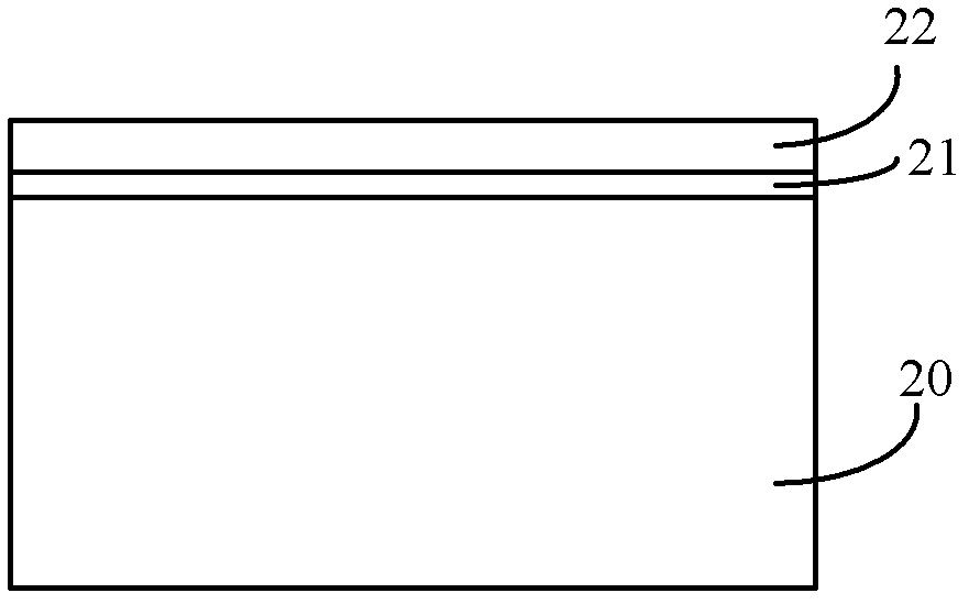
[0055] Please refer to figure 2 A semiconductor substrate 20 is provided, an oxide pad layer 21 is formed on the surface of the semiconductor substrate 20 , and a hard mask layer 22 is formed on the surface of the oxide pad layer 21 .

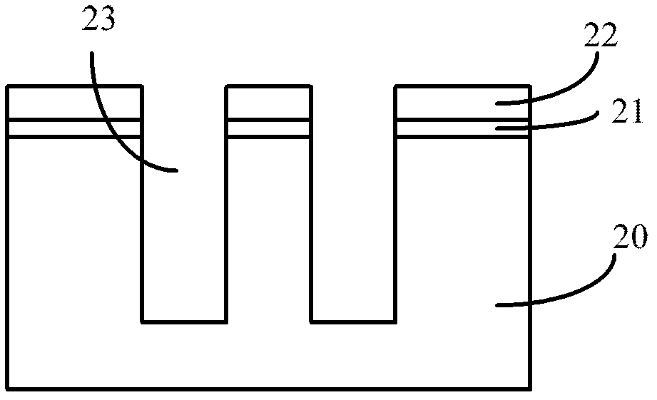
[0056] Please refer to image 3 , pattern the hard mask layer 22 and the oxide liner layer 21 , and use the patterned hard mask layer 22 and the oxide liner layer 21 as a mask to etch the semiconductor substrate 20 to form trenches 23 .

[0057] The formation process for forming the trench 23 is: dry etching or wet etching, preferably dry etching, because of its anisotropy, the shape of the trench 23 can be precisely formed.

[0058]However, the etching process is likely to cause lattice damage to the surface of the semiconductor substrate 20, thereby affecting the progress of the subsequent process and further affecting...


PUM


Abstract

The invention provides a method for forming a fin portion of a fin field effect tube and the fin field effect tube. The method for forming the fin portion of the fin field effect tube includes the steps: providing a semi-conductor substrate, forming a silicon oxide layer on the surface of the semi-conductor substrate, and forming a hard mask layer on the surface of the silicon oxide layer; etching the silicon oxide layer and the hard mask layer, forming a fin portion groove and exposing the semi-conductor substrate; filling the fin portion groove with a polycrystal material or an amorphous semi-conductor material; forming the fin portion in the fin portion groove with the polycrystal material or the amorphous semi-conductor material through an epitaxial growth method; conducting smoothening with the surface of the hard mask layer as a termination position; and removing the hard mask layer and exposing the silicon oxide layer. Crystal lattice damage on the surface of the formed fin portion is reduced, the fin portion and the inside of the silicon oxide layer are compact and free of gaps, the height of the fin portion is controllable, the performance and reliability of the fin field effect tube are improved, and forming process of small semi-conductor devices is precise.

Description

technical field [0001] The invention relates to the technical field of semiconductors, in particular to a method for forming a fin of a fin field effect transistor and a method for forming a fin field effect transistor. Background technique [0002] With the continuous development of semiconductor process technology and the gradual reduction of process nodes, gate-last (gate-last) process has been widely used to obtain an ideal threshold voltage and improve device performance. However, when the feature size (CD, Critical Dimension) of the device is further reduced, even if the gate-last process is adopted, the structure of the conventional MOS field effect transistor can no longer meet the requirements for device performance, and the multi-gate device has been obtained as a substitute for the conventional device. Widespread concern. [0003] Fin Field Effect Transistor (Fin FET) is a common multi-gate device, such as figure 1 Shown is a three-dimensional structure of a fin...

Claims


Application Information

Patent Timeline
IPC IPC(8): H01L21/28H01L21/336
Inventor 宋化龙
Owner SEMICON MFG INT (SHANGHAI) CORP
Why Eureka
Try Eureka