

Optical material high temperature transmittance testing device
A technology of optical materials and testing devices, which is applied in the direction of transmittance measurement, etc., can solve the problems of light transmittance decrease, transmittance characteristics deterioration, and inability to reflect material transmittance characteristics, etc., to improve measurement accuracy, good The effect of temperature uniformity
- Summary
- Abstract
- Description
- Claims
- Application Information
AI Technical Summary
Problems solved by technology
Method used
Image

Examples
Embodiment Construction
[0027] The present invention will be further described below in conjunction with the accompanying drawings and preferred embodiments.
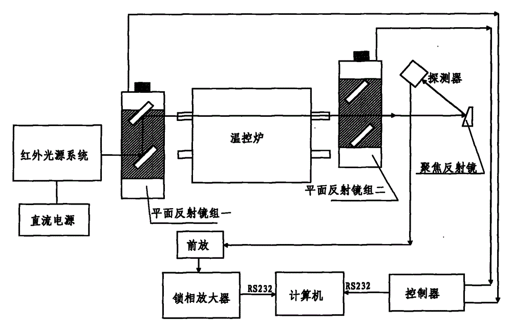
[0028] as figure 1 As shown, the high-temperature transmittance measuring instrument of the preferred embodiment of the present invention is composed of an infrared light source system, a plane mirror group 1, a precision temperature-controlled furnace, a plane mirror group 2, a focusing mirror, a photoelectric detection processing system, and a computer.
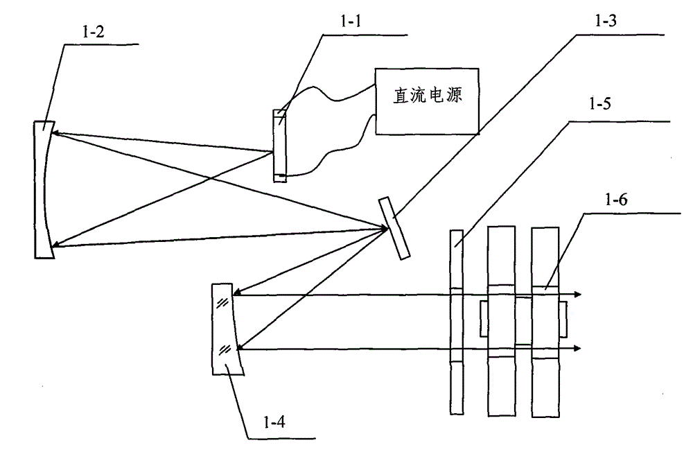
[0029] according to figure 2 As shown, the infrared light source system includes an infrared light source 1-1, a collimating mirror 1-4, an imaging lens 1-2, a plane mirror 1-3, a chopper 1-5, a filter group 1-6, and an infrared light source 1-1 is a silicon carbide rod lamp, and collimating mirror 1-4 is an off-axis parabolic reflector. The silicon carbon rod lamp is powered by a DC precision steady current source to provide continuous infrared light. The infrared light beam emitted by...
PUM
| Property | Measurement | Unit |
|---|---|---|
| Wavelength range | aaaaa | aaaaa |
Abstract
Description
Claims
Application Information