

Method for preparing metal chalcogenide film
A metal chalcogenide and thin film technology, which is applied in metal material coating process, gaseous chemical plating, coating, etc., can solve the problem that the thickness of molybdenum disulfide thin film is difficult to control accurately, randomness limits large-scale integrated production, size , position and thickness are uncontrollable, etc., to achieve the effect of simple method, good crystal quality and good electrical properties
- Summary
- Abstract
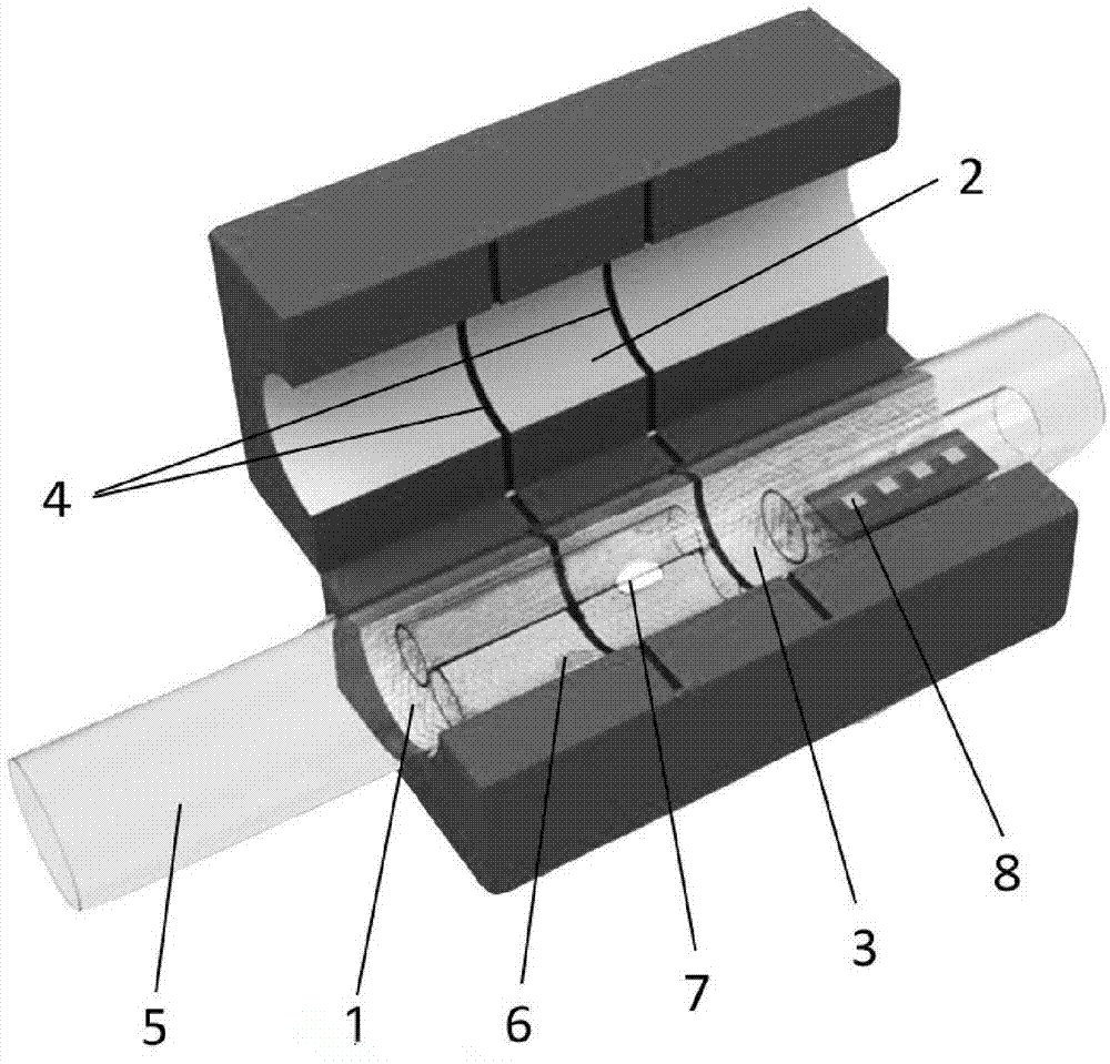
- Description
- Claims
- Application Information
AI Technical Summary
Problems solved by technology
Method used
Image

Examples
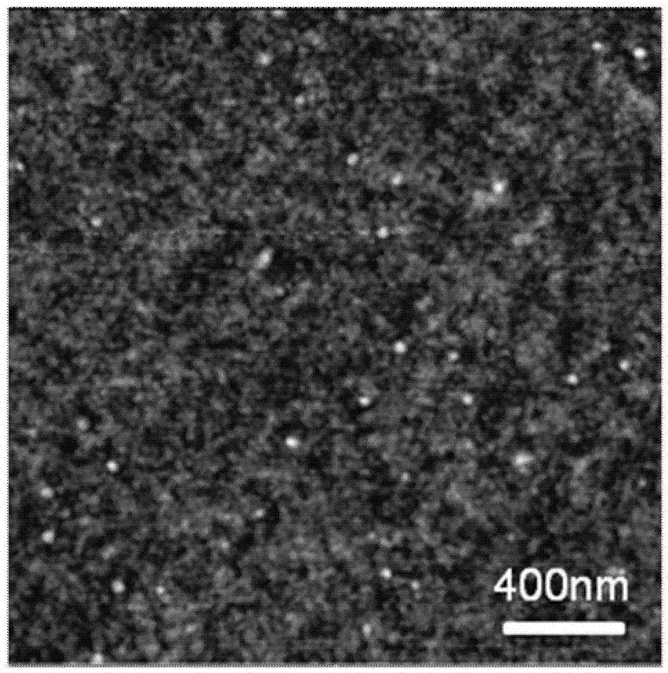
Embodiment 1
[0058] The sulfur powder and molybdenum trioxide are 30mg and 0.3g respectively, the evaporation temperature is 120°C and 500°C respectively, the deposition temperature of silicon dioxide is 750°C, the air pressure is 1.39torr, and the growth time is 15min.
Embodiment 2
[0060] The sulfur powder and molybdenum trioxide are 50mg and 0.3g respectively, the evaporation temperature is 120°C and 530°C respectively, the deposition temperature of silicon dioxide is 750°C, the air pressure is 1.39torr, and the growth time is 20min.
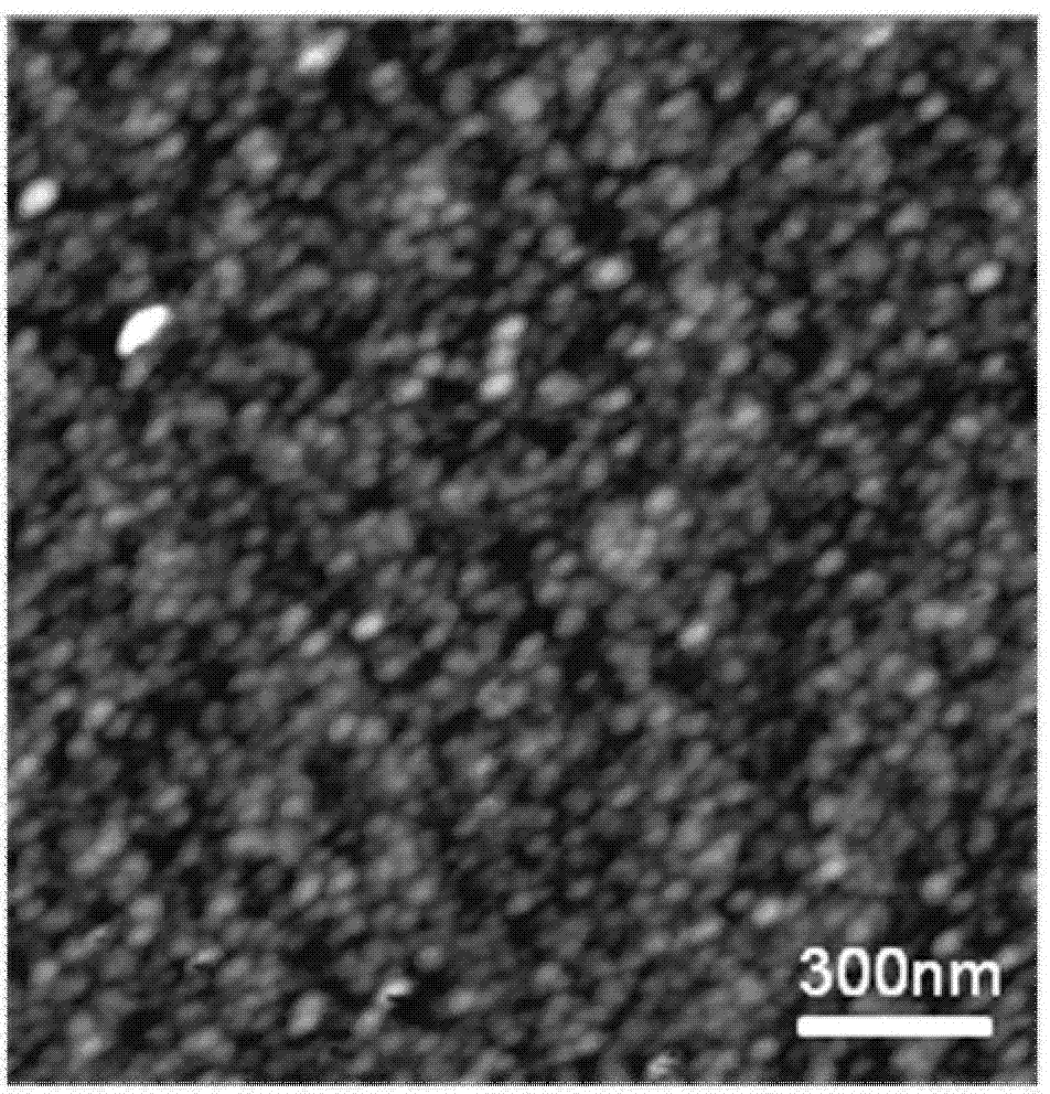
Embodiment 3
[0062] The sulfur powder and molybdenum trioxide are 50mg and 0.4g respectively, the evaporation temperature is 120°C and 530°C respectively, the deposition temperature of silicon dioxide is 750°C, the air pressure is 1.39torr, and the growth time is 40min.
PUM
| Property | Measurement | Unit |
|---|---|---|
| size | aaaaa | aaaaa |
| particle diameter | aaaaa | aaaaa |
Abstract
Description
Claims
Application Information