Titanium nitride chemical vapor deposition device

A titanium nitride chemical and vapor deposition technology, which is applied in the direction of gaseous chemical plating, metal material coating process, coating, etc., can solve the problem that the side wall of the tungsten through hole cannot be treated by plasma, so as to improve the quality, Expand the effect of filling the space

Inactive Publication Date: 2013-07-10
SHANGHAI HUALI MICROELECTRONICS CORP
View PDF4 Cites 1 Cited by
  • Summary
  • Abstract
  • Description
  • Claims
  • Application Information

AI Technical Summary

Problems solved by technology

[0004] The invention provides a titanium nitride chemical vapor deposition equipment to solve the problem in the prior art that the side wall of the tungsten through hole cannot be treated by plasma during the titanium nitride chemical vapor deposition process

Method used


Image

  • Titanium nitride chemical vapor deposition device
  • Titanium nitride chemical vapor deposition device

Examples


Embodiment Construction

[0014] In order to describe the technical solution of the above invention in more detail, specific examples are listed below to demonstrate the technical effect; it should be emphasized that these examples are used to illustrate the present invention and not limit the scope of the present invention.

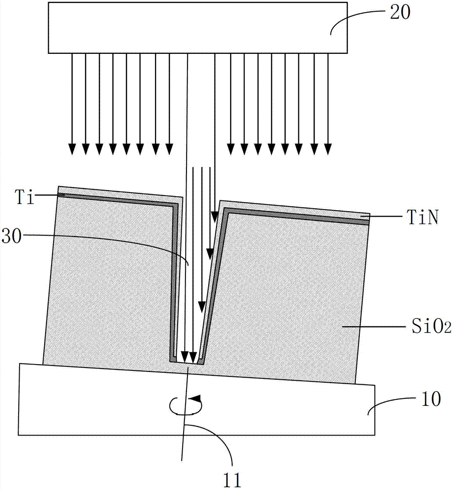
[0015] Titanium nitride chemical vapor deposition equipment provided by the invention, such as figure 2 As shown, it includes a base 10 for carrying a silicon wafer and a shower head 20 arranged on the upper end of the silicon wafer. Specifically, the bottom layer of the silicon wafer in this embodiment is SiO2, then a layer of Ti is deposited, and finally tetradimethyl Aminopeptide (TDMAT) is used as the initial compound to form a layer of TiN, and the silicon wafer contains tungsten through holes 30, nitrogen and hydrogen gas injected from the shower head 20 are injected into the tungsten through holes 30 to perform plasma on the TiN deal with. The included angle between the ...


PUM


Abstract

The invention relates to a titanium nitride chemical vapor deposition device which comprises a base used for bearing a silicon wafer, and a spray head arranged at the upper end of the silicon wafer, wherein the included angle formed between the plane on which the upper surface of the base is arranged and the spraying direction of the spray head is 60-89 degrees; the titanium nitride chemical vapor deposition device also comprises a driving part which is connected with the base; and the driving part is used for driving the base to rotate around a rotating shaft which is vertical to the upper surface the base. The base is arranged in an inclined way, so that the side wall at the lower side of a tungsten through hole can be fully contacted with plasma, and the plasma can be treated; and furthermore, the base can be driven to rotate by the driving part, so that all the side walls of the tungsten through hole can be fully contacted with the plasma, so that the filling space of tungsten is enlarged, and the quality of the silicon wafer is improved.

Description

technical field [0001] The invention relates to the field of semiconductor manufacturing, in particular to a titanium nitride chemical vapor deposition equipment. Background technique [0002] In the semiconductor process, an integrated circuit (IC, English full name: integrated circuit) often includes millions of electronic devices. With the development of planarization and thinning, tens of thousands to millions of transistors will be integrated on silicon wafers of only a few millimeters square in ultra-large-scale integrated circuits. [0003] With the further shrinking of the device size, its manufacturing process requirements are also undergoing major challenges. Among them, especially in the field of tungsten vias (contact), as the characteristic size (CD, English full name: characterized dimension) continues to shrink, the space that tungsten can fill is getting smaller and smaller. In order to better fill tungsten, The thickness control of the tungsten barrier lay...

Claims


Application Information

Patent Timeline
Patent Type & Authority Applications(China)
IPC IPC(8): C23C16/34C23C16/458
Inventor 周军
Owner SHANGHAI HUALI MICROELECTRONICS CORP
Why Eureka
Try Eureka