Manufacturing method of thin-film capacitor and thin-film capacitor obtained through manufacturing method

A technology of film capacitors and manufacturing methods, applied in the direction of film/thick film capacitors, fixed capacitor dielectrics, laminated capacitors, etc., can solve the problems of insulation withstand voltage drop, leakage current increase, etc., to suppress the generation of hillocks, leakage Excellent current characteristics and insulation withstand voltage characteristics

Inactive Publication Date: 2013-07-10
MITSUBISHI MATERIALS CORP
View PDF4 Cites 3 Cited by
  • Summary
  • Abstract
  • Description
  • Claims
  • Application Information

AI Technical Summary

Problems solved by technology

As a result, when a capacitor is formed, the leakage current between the upper electrode and the lower electrode also increases, and the insulation withstand voltage also decreases.

Method used


Image

  • Manufacturing method of thin-film capacitor and thin-film capacitor obtained through manufacturing method
  • Manufacturing method of thin-film capacitor and thin-film capacitor obtained through manufacturing method

Examples


Embodiment 1

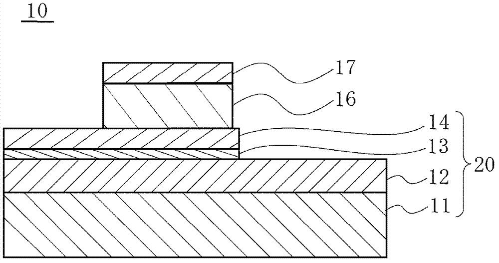
[0046] First, if figure 1 As shown, an insulator film 12 is formed on a substrate 11 . Specifically, a 500-nm-thick SiO 2 membrane. Secondly, by sputtering method on the above SiO 2 A metal Ti film was formed on the film, and heat-treated at 700° C. for 1 minute to form an adhesion layer 13 with a thickness of 30 nm.

[0047] Next, using Pt as a noble metal material, a lower electrode 14 with a thickness of 100 nm was formed on the above-mentioned adhesion layer 13 by a sputtering method. The crystal orientation in the lower electrode 14 is formed to be preferentially oriented to the (111) plane. In addition, the average crystal grain size in the lower electrode 14 was adjusted to 40 nm. Thus, a support body 20 composed of the substrate 11 , the insulator film 12 formed on the substrate 11 , and the lower electrode 14 formed on the insulator film 12 via the adhesive layer 13 is obtained.

[0048] Next, a thin film forming precursor solution is prepared. Specifically, fi...

Embodiment 2

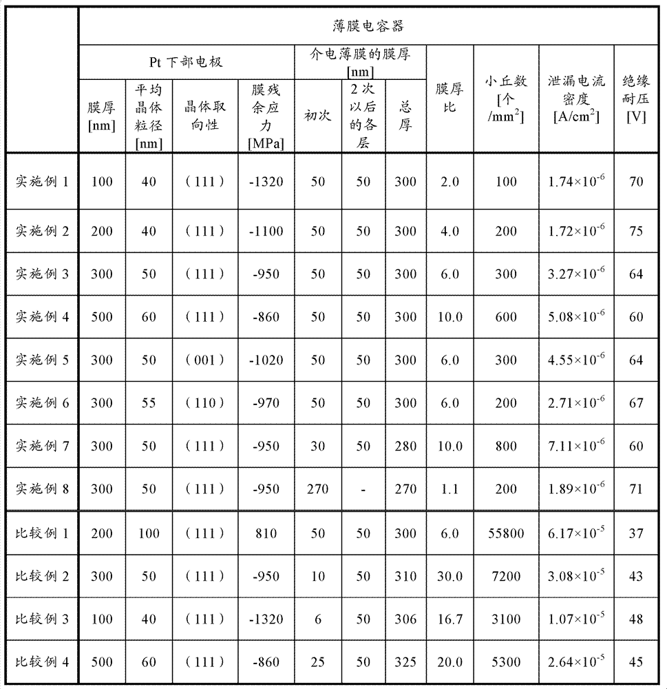
[0052] A film capacitor was obtained in the same manner as in Example 1 except that a dielectric film was formed on the lower electrode having a thickness of 200 nm and a residual stress of the value shown in Table 1 below. This film capacitor was referred to as Example 2.

Embodiment 3

[0054] A film capacitor was obtained in the same manner as in Example 1 except that a dielectric thin film was formed on the lower electrode having a thickness of 300 nm and an average crystal grain size and residual stress as shown in Table 1 below. This film capacitor was referred to as Example 3.


PUM

PropertyMeasurementUnit
Average crystal sizeaaaaaaaaaa
Residual stressaaaaaaaaaa
Thicknessaaaaaaaaaa

Abstract

The invention discloses a manufacturing method of a thin-film capacitor. Small protrusions which are the reasons of decreasing of various characteristics in the thin-film capacitor are restricted, and the thin-film capacitor with a good leakage current characteristic and a good insulation and voltage resistance characteristic is manufactured. According to the manufacturing method of the thin-film capacitor, after a lower portion electrode is formed, an annealing process with temperature higher than 300 DEG C is not conducted, a thin film forms a precursor solution which is coated on the lower portion electrode, drying is conducted with a preset temperature in a range of a room temperature to 450 DEG C, sintering is conducted with a preset temperature in a range of 450-800 DEG C which is higher than the drying temperature, in the process from the coating to the sintering, once or more than twice processes from the coating to the sintering are conducted, or after more than twice processes from the coating to the sintering are conducted, once sintering is conducted, and the thickness of the dielectric thin film which is formed after primary sintering is arranged to be 20-600mm. preferably, a ratio (the thickness of the lower portion electrode / the thickness of the dielectric thin film) of the thickness of the lower portion electrode and the thickness of the dielectric thin film formed after the primary sintering is in a range of 0.10-15.0.

Description

technical field [0001] The present invention relates to a method of manufacturing a film capacitor excellent in leakage current characteristics and insulation withstand voltage characteristics. In more detail, it relates to a method of manufacturing these film capacitors by suppressing hillocks generated in the manufacturing process of film capacitors and preventing the increase in leakage current density and the decrease in dielectric breakdown voltage caused thereby. A method of producing film capacitors with excellent properties. Background technique [0002] Electronic devices such as DRAM (Dynamic Random Access Memory), FeRAM (Ferroelectric Random Access Memory), and RF circuits have capacitors that function as capacitors (condensers). , the area that the capacitor can occupy within the device also tends to be narrower. A capacitor has a basic structure in which an upper electrode, a lower electrode, and a dielectric layer are sandwiched between the two electrodes. Th...

Claims


Application Information

Patent Timeline
IPC IPC(8): H01G4/33H01G4/12
Inventor 樱井英章渡边敏昭曽山信幸
Owner MITSUBISHI MATERIALS CORP
Why Eureka
Try Eureka