

Epitaxial growth structure in GaN base green-light light emitting diode (LED) with P-type GaN
An epitaxial growth, green-based technology, applied in the direction of electrical components, circuits, semiconductor devices, etc., can solve problems such as downward bending, affecting crystal quality and radiation recombination efficiency, fragmentation, etc.
- Summary
- Abstract
- Description
- Claims
- Application Information
AI Technical Summary
Problems solved by technology
Method used
Image

Examples
Embodiment Construction
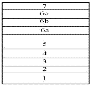
[0010] figure 1 Among them, 1 is the sapphire substrate, 2 is the GaN nucleation layer, 3 is the undoped GaN layer, 4 is the n-type GaN layer, 5 is the InGaN / GaN multi-quantum well active layer, and 6(a) is the low-temperature P-type GaN hole injection layer, 6(b) is a P-type Al(In)GaN electron blocking layer, 6(c) is a P-type GaN hole activation layer, and 7 is an InGaN current tunneling layer.
[0011] from figure 1 It can be seen that a GaN nucleation layer 2, an undoped GaN layer 3, an n-type GaN layer 4, an InGaN / GaN multi-quantum well active layer 5, a P-type GaN, and a low-temperature P-type GaN hole are grown sequentially on the substrate 1. Injection layer 6(a), P-type Al(In)GaN electron blocking layer 6(b), P-type GaN hole activation layer 6(c), and InGaN current tunneling layer 7.
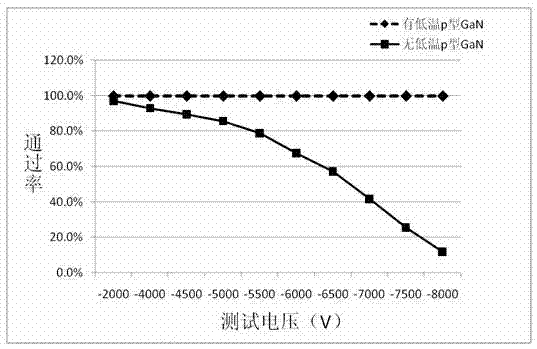
[0012] from figure 2 It can be seen that the ESD test yield rate of LEDs with low-temperature p-type GaN is still 100% when the reverse voltage is 8000V, while the ESD test pass rate...
PUM
 Abstract
Description
Claims
Application Information