A production method for an electroformed stencil with mark points

A production method and positioning point technology, which are applied in the preparation of printing surface, photoengraving process of pattern surface, printing and other directions, can solve the problems that the precision and quality of the opening of the steel mold cannot meet the requirements well, and the quality of the board surface is not high enough.

Inactive Publication Date: 2013-07-17
KUN SHAN POWER STENCIL
View PDF5 Cites 2 Cited by
  • Summary
  • Abstract
  • Description
  • Claims
  • Application Information

AI Technical Summary

Problems solved by technology

However, the opening accuracy and quality of the steel mold made by traditional technology through laser cutting technology cannot meet the requirements well, and the quality of the board surface is not high enough.

Method used


Image

  • A production method for an electroformed stencil with mark points
  • A production method for an electroformed stencil with mark points
  • A production method for an electroformed stencil with mark points

Examples


Embodiment 1

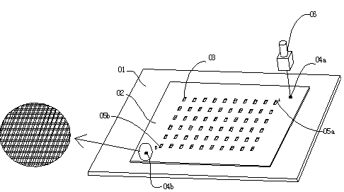
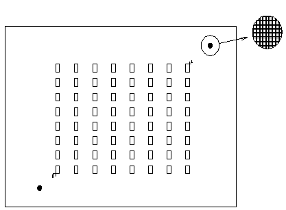
[0067] In order to better align with the PCB accurately and transfer an accurate amount of material to an accurate position, the electroforming process is used to make the electroforming stencil. The process steps include:

[0068] (1) Pre-treatment of the mandrel: degreasing, pickling and sandblasting the mandrel to remove oil stains and impurities on the surface, and smooth the surface;

[0069] (2) Film: apply film to the surface of the mandrel;

[0070] (3) Exposure: Expose the pattern opening area so that the unexposed area can be removed by development, leaving the exposed part as a protective film for the subsequent electroforming step;

[0071] (4) Single-sided development: develop the unexposed part in step (3), leaving the exposed part as a protective film for the subsequent electroforming step;

[0072] (5) Electroforming: The electroforming method is used to electroform the electroforming material to the exposure area;

[0073] (6) Fading film: remove the exposed...

Embodiment 2

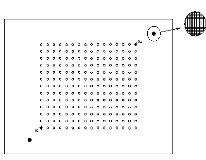
[0086] In order to better align with the PCB accurately and transfer an accurate amount of material to an accurate position, the electroforming process is used to make the electroforming stencil. The process steps include:

[0087] (1) Pre-treatment of the mandrel: degreasing, pickling and sandblasting the mandrel to remove oil stains and impurities on the surface, and smooth the surface;

[0088] (2) Film: apply film to the surface of the mandrel;

[0089] (3) Exposure: Expose the pattern opening area so that the unexposed area can be removed by development, leaving the exposed part as a protective film for the subsequent electroforming step;

[0090] (4) Single-sided development: develop the unexposed part in step (3), leaving the exposed part as a protective film for the subsequent electroforming step;

[0091] (5) Electroforming: The electroforming method is used to electroform the electroforming material to the exposure area;

[0092] (6) Fading film: remove the exposed...


PUM

PropertyMeasurementUnit
thicknessaaaaaaaaaa
evennessaaaaaaaaaa

Abstract

The present invention relates to a production method for an electroformed stencil with mark points, including the production of the electroformed stencil and the production of the mark points. The production method is characterized by comprising the steps of: placing the fixed electroformed stencil on a cutting base platform; selecting any two openings diagonally positioned on the electroformed stencil, reading coordinates of specific points of the openings, positioning the electroformed stencil through the coordinates of specific points, and determining coordinates of the mark points via comparing with an original file; adjusting cutting parameters and the vertical height of a laser cutting head to enable a laser focus to fall on the surface of the electroformed stencil; and emitting laser light through the laser cutting head to perform cutting at the mark point area on the surface of the electroformed stencil. According to the production method for the electroformed stencil with mark points, the obtained electroformed stencil has good surface quality, no pinholes or pittings, thereby improving printing quality; and the mark points have high positioning accuracy, and relatively high degrees of recognition, improving alignment accuracy of a PCB with the electroformed stencil.

Description

[0001] technical field [0002] The invention relates to a method for manufacturing a live electroformed stencil, in particular to a method for manufacturing an electroformed stencil with positioning points. [0003] Background technique [0004] With the pursuit of miniaturization of electronic products, the perforated plug-in components used before can no longer be reduced; the functions of electronic products are more complete, and the integrated circuits (ICs) used can no longer perforate components, especially large-scale and highly integrated ICs, which have to use surface SMT components, so the stencil printing process has developed rapidly in the electronics manufacturing industry, and SMT printing is a typical example. The production of the template is not only the first step in the SMT assembly process, but also the most important step. The main function of the stencil is to aid in the deposition of solder paste, transferring the exact amount of material to the e...

Claims


Application Information

Patent Timeline
Patent Type & Authority Applications(China)
IPC IPC(8): B41C1/14B41N1/04B41N3/00G03F7/00
Inventor 魏志凌高小平赵录军
Owner KUN SHAN POWER STENCIL
Why Eureka
Try Eureka