Three-dimensional mask plate for printing

A three-dimensional, masking technology, applied in printing, printing machines, printing processes, etc., can solve the problems of small printing effective area, poor printing effect, deviation transfer of transfer materials, etc.

Inactive Publication Date: 2013-07-17
KUN SHAN POWER STENCIL
View PDF15 Cites 6 Cited by
  • Summary
  • Abstract
  • Description
  • Claims
  • Application Information

AI Technical Summary

Problems solved by technology

In the field of high-precision manufacturing, even small convex and concave parts on the surface of the substrate will cause large deviations in positional accuracy and dimensional accuracy during the transfer process and deformation of the mask, resulting in scrapping of products and masks
When using two-dimensional mask transfer, the mask opening at the edge of the concave-convex area on the substrate surface cannot be precisely aligned because it cannot be in close contact with the substrate, resulting in deviation transfer or dislocation transfer of the transfer material
In the prior art, pad printing is often used for non-planar printing, but pad printing has problems such as small printing effective area and poor printing effect, especially for large-area printing products that cannot meet its requirements, and requires equipment Large investment and high cost
Therefore, the traditional pad printing method can no longer meet the current requirements for screen printing of special-shaped products

Method used


Image

  • Three-dimensional mask plate for printing
  • Three-dimensional mask plate for printing
  • Three-dimensional mask plate for printing

Examples


Embodiment 1

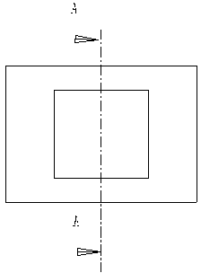
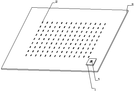
[0032] combine Figure 1A , 1B , figure 2 and 3 As shown, the embodiment of the present invention provides a three-dimensional mask 11 for printing, including a substrate, a printing surface 3 and a PCB surface 4 located on both sides of the substrate, the mask 11 has a plurality of graphic openings 22 and a three-dimensional structure. The three-dimensional structure includes a raised area 1 on the printing surface 3 and a recessed area 2 on the PCB surface 4 . The three-dimensional nickel metal mask 11 for high-precision printing can be obtained, with good surface brightness, good coating surface quality, no pitting, pinholes, etc.; up and down areas of different heights or depths can be obtained, and the up and down areas are the same as The outer angle of the board surface is very close to 90°, which is beneficial to the precision requirements of the solder paste during printing; compared with the laser stencil, the opening precision is higher, the opening quality is be...

Embodiment 2

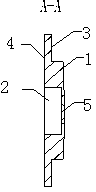
[0040] The difference from the above-mentioned Embodiment 1 is that the combination Figure 4As shown, the three-dimensional structure of the mask plate 11 is provided with a pattern opening 5 that meets the printing requirements, and the area corresponding to the opening 5 of the PCB board is provided with a soldering copper stage 333 . The graphic opening 5 on the three-dimensional three-dimensional structure is an opening with a small upper part and a large lower part, and its taper is 3-8°.

[0041] It can be seen from the above embodiments that the embodiment of the present invention provides a three-dimensional mask plate 11 for printing, which includes a substrate, a printing surface 3 and a PCB surface 4 located on both sides of the substrate, and the mask plate 11 has a plurality of pattern openings 22 and 4. The three-dimensional structure includes a raised area 1 on the printing surface 3 and a recessed area 2 on the PCB surface 4 . The mask 11 has three-dimensiona...


PUM


Abstract

The invention discloses a three-dimensional mask plate for printing. The three-dimensional mask plate comprises a substrate, and a printing surface and a printed circuit board (PCB) surface, which are arranged on two sides of the substrate, wherein the mask plate is provided with a plurality of graphic openings and a three-dimensional structure, the three-dimensional structure comprises a projection area which is arranged on the printing surface and a concave area which is arranged on the PCB surface. The mask plate is provided with the three-dimensional projection part and the three-dimensional concave part, the height of the projection is 0.1mm to 10mm, the concave depth is 0.1mm to 10mm, and angles formed between the projection part and the plate surface and between the concave part and the plate surface are 80 to 90 DEG; the mask plate is made of pure nickel, and the precision is high; the uniformity is high, the quality is good, and high brightness, no rough spot, no scratch and no pin hole can be realized; and the opening quality is good, and the wall is smooth and free from burrs; and the mask plate is low in production cost, simple in process and low in energy consumption.

Description

technical field [0001] The invention relates to a three-dimensional mask, in particular to a three-dimensional mask for printing. Background technique [0002] With the rapid development of my country's electronics industry, stencil printing technology has also been applied in the electronics manufacturing industry, and SMT printing is a typical example. In the manufacturing process of electronic products, soldering electronic components and PCB needs to put tin on the PCB first, and there are hundreds of pads on the PCB that need to be tinned. The position of each pad corresponds to the electronic component. The best way to accurately tin the pads that need to be tinned at one time is to print. The usual method used in the electronics manufacturing industry is to make a stainless steel sheet with numerous small holes, each hole corresponds to a pad that needs to be tinned, and then paste the stainless steel sheet on the stretched mesh, and the mesh is pasted. On the under...

Claims


Application Information

Patent Timeline
Patent Type & Authority Applications(China)
IPC IPC(8): B41F15/36
CPCB41F15/34H01L51/0004B41N1/24H05K3/1225H05K3/3485H10K71/13H05K3/12
Inventor 魏志凌高小平
Owner KUN SHAN POWER STENCIL
Why Eureka
Try Eureka