Preparation method and device of phosphorus-doped nano silicon material

A nano-material and nano-silicon technology, which is applied in the direction of silicon, can solve the problems of uneven size of nanoparticles, low production capacity of nanoparticles, and difficulty in avoiding cross-contamination of chemical components, so as to increase the area, improve the uniformity, and increase the production capacity. Effect

Inactive Publication Date: 2013-07-31
苏州金瑞晨科技有限公司
View PDF4 Cites 4 Cited by
  • Summary
  • Abstract
  • Description
  • Claims
  • Application Information

AI Technical Summary

Problems solved by technology

It is characterized by low cost and high yield, but it is difficult to avoid cross-contamination of various chemical components in the synthesis process
[0006] The commonly used spark discharge method to prepare nanoparticles cannot control the distance between the electrode raw materials, which leads to the inability to control the spark discharge process, making the prepared nanoparticles uneven in size, most of the prepared particles are in the micron range, and the actual nanoparticle production capacity not tall

Method used


Image

  • Preparation method and device of phosphorus-doped nano silicon material
  • Preparation method and device of phosphorus-doped nano silicon material

Examples


Embodiment Construction

[0033] The technical solution of the present invention will be further described below in conjunction with the accompanying drawings and four preferred embodiments.

[0034] Device example:

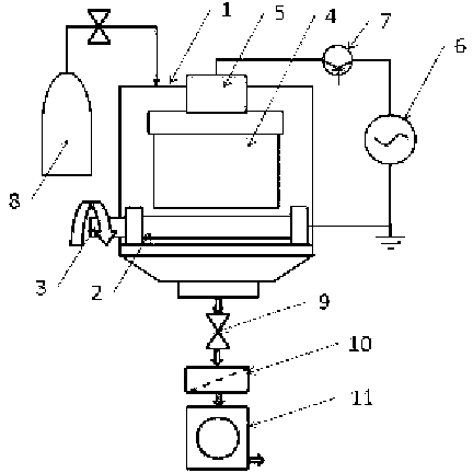
[0035] like figure 1 and figure 2 Shown: a device for preparing nanoparticles by controllable spark discharge, including a cavity 1 for accommodating spark discharge, one end of the cavity 1 is connected to a pipeline for a dielectric material 8 to enter, and the other end is connected to a particle collector through a valve 9 10. It also includes a first electrode 2 placed in the cavity 1, a second electrode 4, and a power supply 6 connected to the first electrode 2 and the second electrode 4; the first electrode 2 is connected with a A rotating rotary motor 3, the second electrode 4 is connected with a stepper motor 5 that moves the second electrode 4 back and forth.

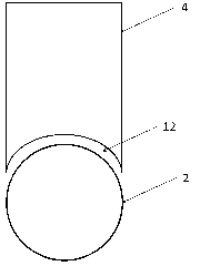
[0036] The first electrode 2 is a block of nanomaterials to be prepared, and the shape is a cylinder.

[0037] The s...


PUM

PropertyMeasurementUnit
diameteraaaaaaaaaa
diameteraaaaaaaaaa
lengthaaaaaaaaaa

Abstract

The invention discloses a preparation method and device of a phosphorus-doped nano silicon material. The method comprises the following steps: arranging a bar-shaped raw material used as an electrode material in a spark discharge chamber; under the protection of a dielectric gas or liquid material, applying a voltage onto the raw material of the electrode through a pulse power source, and generating a spark to locally melt and gasify the raw material of the electrode; injecting the molten and gasified raw material of the electrode into the dielectric gas or liquid to form nano particles; and then, separating and collecting through a particle collecting device containing a filter cloth. According to the method and device, the spark discharge area of the raw material of the electrode can be increased, so that the productivity of the nano particle preparation is increased and meets the requirements for large-scale production; and the spacing between raw materials of electrodes can be controlled, thereby controlling the size of the formed nano particles and enhancing the uniformity of particle size distribution.

Description

technical field [0001] The invention belongs to the technical field of nanomaterials, and in particular relates to a device and method for preparing phosphorus-doped nano-silicon material by using a controllable spark discharge method. Background technique [0002] Nanoparticles, especially semiconductor nanoparticles, such as silicon nanoparticles, have a very wide range of applications in the fields of electronics, optoelectronics, solar energy and biomedicine. For example, as the anode material of lithium battery, silicon nanoparticles can store up to 4.4 lithium atoms per silicon atom, enabling the storage capacity to reach 4200mAHg -1 Theoretical value, much higher than the storage capacity of the current graphite anode 370mAHg -1 . For another example, the printed electronic ink based on silicon nanoparticles has gradually changed the preparation process of semiconductor devices, solar devices, optical, electrical, magnetic and various biomedical sensor devices, from...

Claims


Application Information

Patent Timeline
Patent Type & Authority Applications(China)
IPC IPC(8): C01B33/02
Inventor 刘国钧沈晓东唐云俊周卫卫
Owner 苏州金瑞晨科技有限公司
Why Eureka
Try Eureka