A doping structure to improve the modulation efficiency of depletion-mode silicon-based electro-optic modulators

An electro-optic modulator and modulation efficiency technology, applied in the field of doped structures, can solve the problems of increased carrier absorption loss and difficulty, and achieve the effects of increasing overlap integral, reducing absorption loss, and reducing concentration

Inactive Publication Date: 2016-05-18
INST OF SEMICONDUCTORS - CHINESE ACAD OF SCI
View PDF7 Cites 0 Cited by
  • Summary
  • Abstract
  • Description
  • Claims
  • Application Information

AI Technical Summary

Problems solved by technology

The method of increasing the doping concentration can improve the modulation efficiency to a certain extent. However, according to the plasmonic dispersion effect, high doping concentration will lead to an increase in carrier absorption loss. High absorption loss also has a very adverse effect on the device. Higher requirements will be placed on light sources and detectors
In order to improve the modulation efficiency, the interdigitated electrode structure with PN junctions staggered is currently more popular, but this structure requires a high-precision overlay process, which is difficult

Method used


Image

  • A doping structure to improve the modulation efficiency of depletion-mode silicon-based electro-optic modulators
  • A doping structure to improve the modulation efficiency of depletion-mode silicon-based electro-optic modulators
  • A doping structure to improve the modulation efficiency of depletion-mode silicon-based electro-optic modulators

Examples


Embodiment Construction

[0024] In order to make the object, technical solution and advantages of the present invention clearer, the present invention will be described in further detail below in conjunction with specific embodiments and with reference to the accompanying drawings.

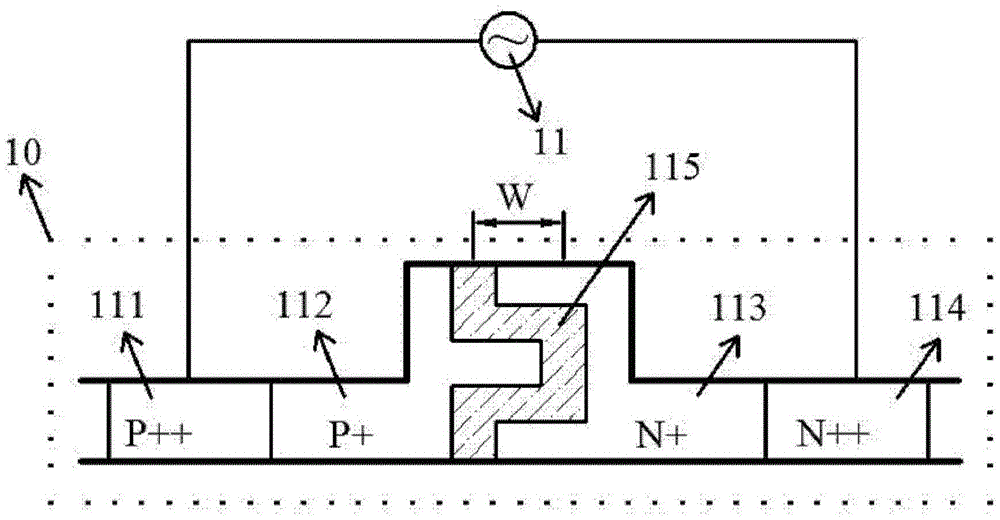
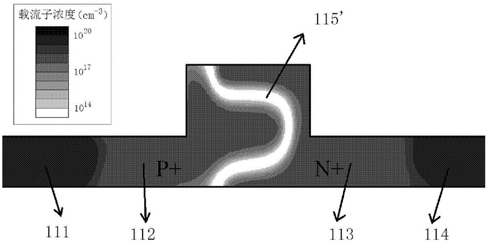
[0025] The doping structure for improving the modulation efficiency of the depletion-type silicon-based electro-optic modulator provided by the present invention uses the carrier dispersion effect for electro-optic modulation. By introducing a non-planar U-shaped waveguide cross-section doping structure, the increase in The overlapping integration of the optical field mode and the carrier depletion region in the waveguide is achieved, and the modulation efficiency is improved compared with the traditional transverse or longitudinal planar doped structure. At the same time, since the impurity doping concentration does not need to be changed, the carrier absorption loss does not increase. On the contrary, due to the increase...


PUM


Abstract

The invention discloses a doping structure capable of improving the modulation efficiency of a depletion silicon-based electrooptical modulator. The doping structure comprises a modulation area waveguide of a silicon-based electrooptical modulator, wherein the waveguide adopts a ridge-shaped optical waveguide structure; a first doping area, a second doping area, a third doping area and a fourth doping area are respectively arranged in the waveguide; a PN node electrical modulation structure shaped like the letter U is formed at the junction between the second doping area and the third doping area; and the first doping area and the fourth doping area are respectively connected with metal wires and connected with a high-frequency driving circuit. When applied to the depletion silicon-based electrooptical modulator, the doping structure can improve the modulation efficiency of the modulator and simultaneously reduce the absorption loss of carriers.

Description

technical field [0001] The invention relates to the technical fields of optical interconnection, high-speed optical modulation, optical switch and the like, in particular to a doping structure for improving the modulation efficiency of a depletion-type silicon-based electro-optic modulator. Background technique [0002] The electro-optical modulator is a key device for realizing electro-optical signal conversion in the optical interconnection system. With the gradual penetration of optical interconnection between circuit boards, between chips and even inside the chip, electro-optic modulators are gradually moving from discrete devices to integration. Silicon-based electro-optic modulators have the characteristics of high integration, low cost, and compatibility with traditional CMOS processes, and have received more and more attention in recent years. [0003] Since silicon is a central inversion symmetric crystal, there is no linear electro-optic effect, and the high-order...

Claims


Application Information

Patent Timeline
Patent Type & Authority Patents(China)
IPC IPC(8): G02F1/025
CPCG02F1/025
Inventor 曹彤彤陈少武
Owner INST OF SEMICONDUCTORS - CHINESE ACAD OF SCI
Why Eureka
Try Eureka