Dye adsorption device, dye adsorption method, and substrate treatment apparatus

A substrate processing device and adsorption device technology, applied in electrolytic capacitors, photovoltaic power generation, electrical components, etc., can solve problems such as impracticality and reduced production efficiency

Inactive Publication Date: 2013-07-31
TOKYO ELECTRON LTD
View PDF5 Cites 2 Cited by
  • Summary
  • Abstract
  • Description
  • Claims
  • Application Information

AI Technical Summary

Problems solved by technology

[0007] The dye adsorption treatment time of the above-mentioned dipping method varies depending on the type of dye, but it takes at least tens of hours. In the manufacturing process of dye-sensitized solar cells, the takt of the entire process is limited. thus becoming a cause of reduced production efficiency
To solve this problem, a method of operating a plurality of dipping-type dye adsorption devices in parallel is considered, but it is not practical to prepare at least dozens of devices.

Method used


Image

  • Dye adsorption device, dye adsorption method, and substrate treatment apparatus
  • Dye adsorption device, dye adsorption method, and substrate treatment apparatus
  • Dye adsorption device, dye adsorption method, and substrate treatment apparatus

Examples


Embodiment approach 1

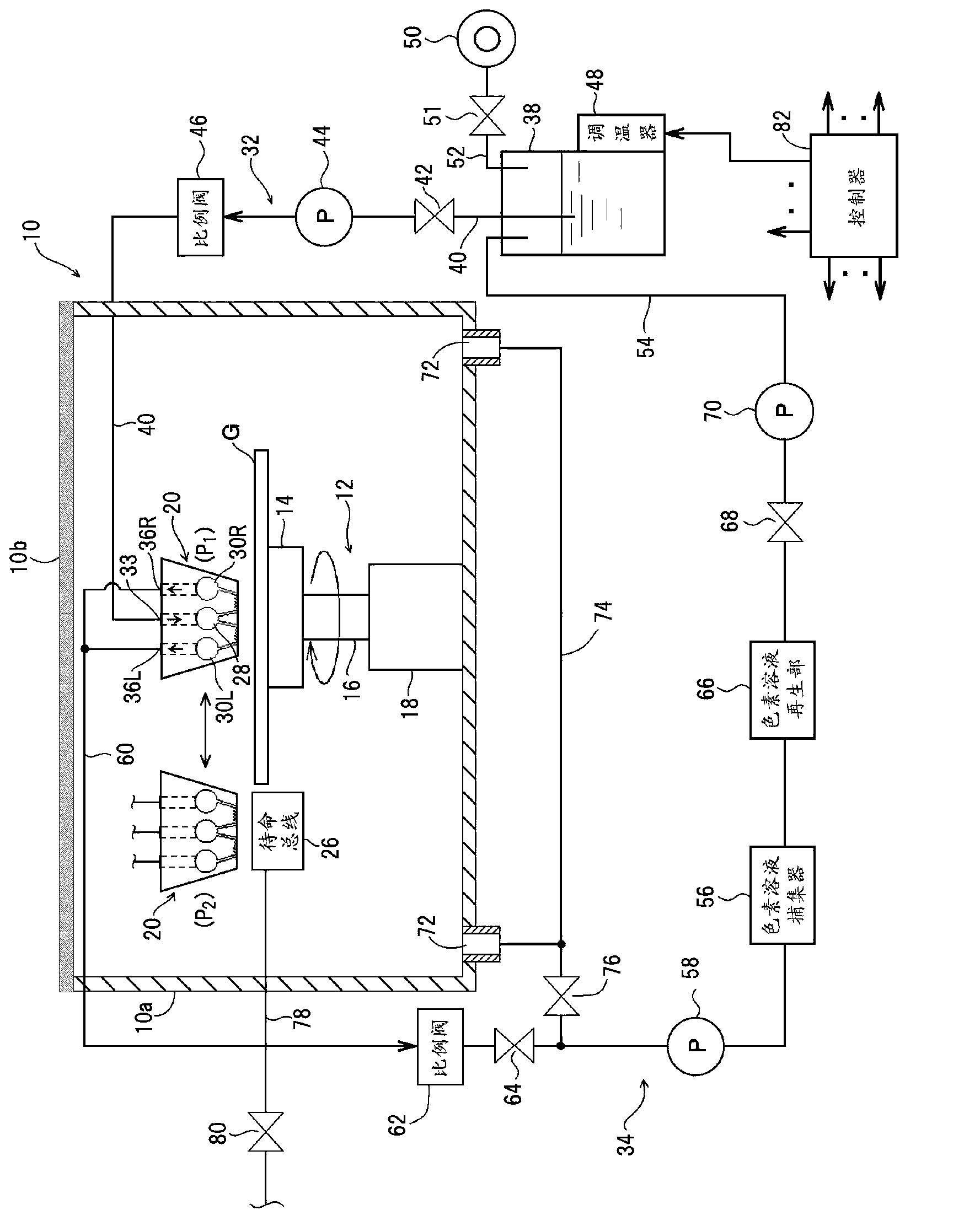
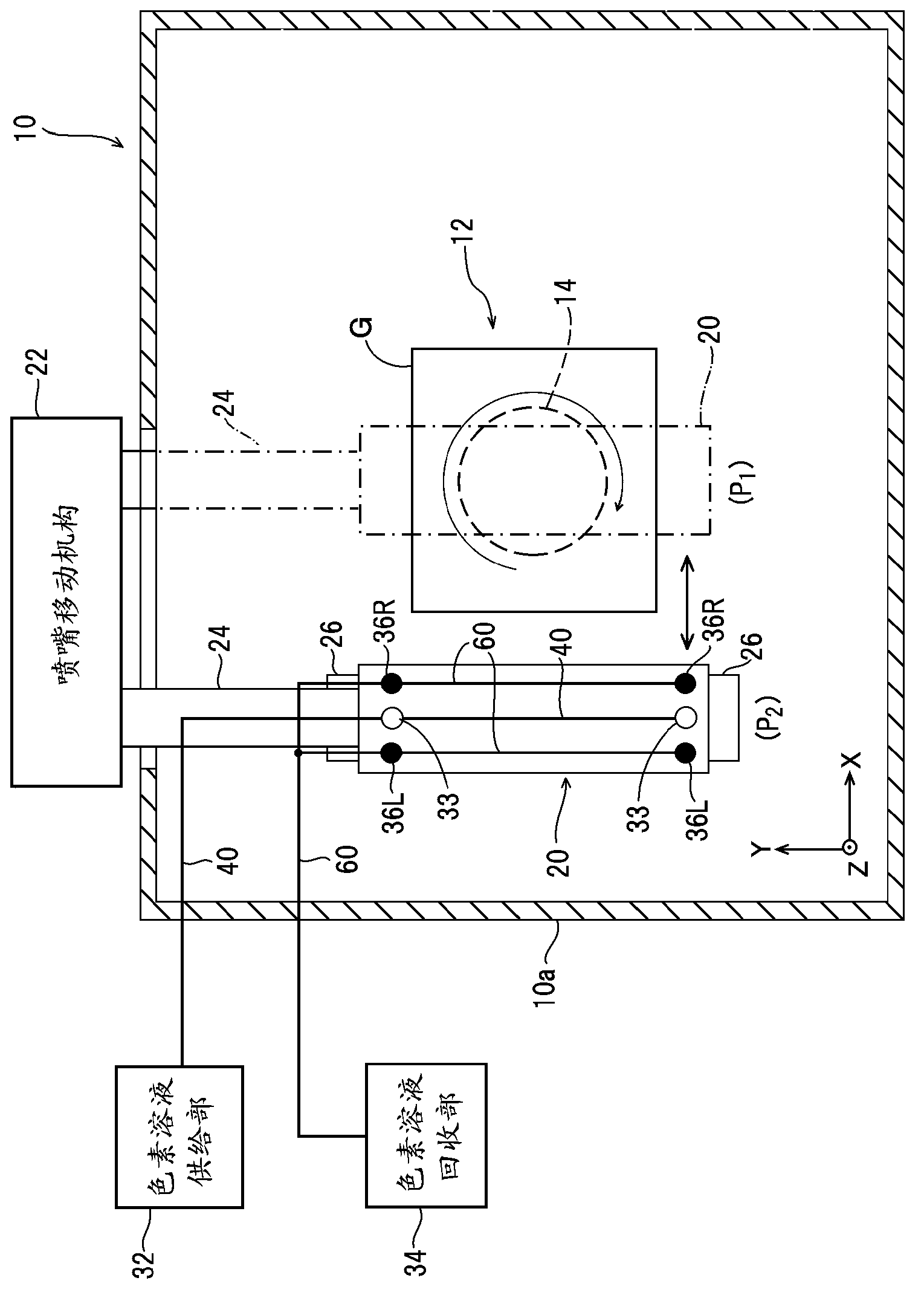
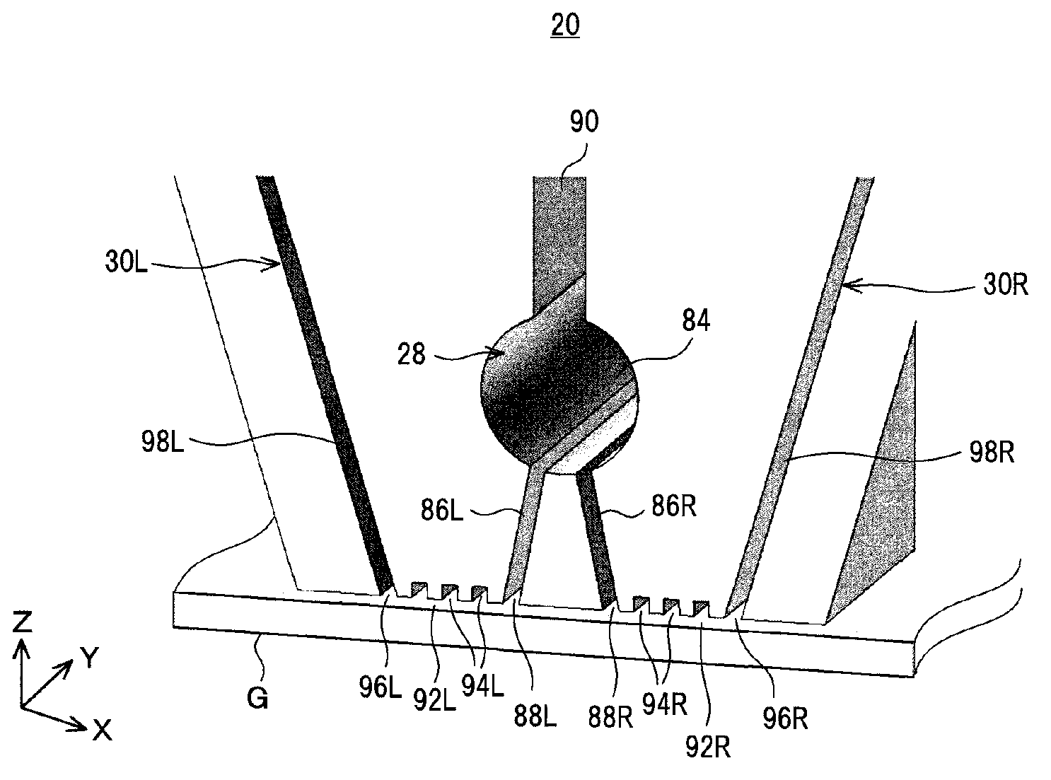
[0045] figure 1 and figure 2 The overall configuration of the dye adsorption device in one embodiment of the present invention is shown in the figure. For example, in the manufacturing process of a dye-sensitized solar cell, the dye adsorption device is used in the step of adsorbing a sensitizing dye to a porous semiconductor layer as a single wafer (leaf). In this case, the transparent substrate 208 on which the transparent electrode 200 and the porous semiconductor layer 204 are formed ( Figure 20 ) as the processed substrate G in the dye adsorption device.

[0046] Wherein, the transparent substrate 208 is made of, for example, transparent inorganic materials such as quartz and glass, or transparent plastic materials such as polyester, acrylic, and polyimide. The transparent electrode 200 is, for example, made of fluorine-doped SnO 2 (FTO), or indium tin oxide (ITO). In addition, the porous semiconductor layer 204 is made of TiO 2 , ZnO, SnO 2 Made of metal oxides....

Embodiment approach 2

[0079] Figure 8 The whole structure of the substrate processing apparatus in one Embodiment of this invention is shown in figure. In the figure, for the above-mentioned first embodiment ( Figure 1 to Figure 7 ) parts with the same configuration or function are given the same reference numerals.

[0080] This substrate processing apparatus fully includes the dye adsorption device in the first embodiment described above as a dye adsorption unit, and further includes a rinse unit and a drying unit. The rinse unit in this embodiment is configured to include a substrate holding unit 12 , a nozzle 20 , a rinse liquid supply unit 110 , and a rinse liquid recovery unit 112 . Among them, the substrate holding unit 12 and the nozzle 20 are used not only in the dye adsorption unit but also in the rinse unit and the drying unit. In addition, the suction pump 58, the vacuum line 60, the electromagnetic proportional valve 62, the electromagnetic on-off valve 64, and the suction pump 58...


PUM


Abstract

[Problem] To significantly reduce processing time of a step of adsorbing dye in a porous semiconductor layer on a substrate surface. [Solution] A flow of a dye solution is formed in a gap between solution guide surface (92L, 92R) of a nozzle (20) and a substrate (G) during the treatment, and a porous semiconductor layer of a treated surface of the substrate is subject to dye adsorption treatment in this flow of the dye solution. Furthermore, impact pressure from slit-like discharge openings (88L, 88R) and pressure of turbulent flow in groove-like uneven sections (92L, 92R) act in the vertical direction in addition to the flow of the dye solution. Thus, aggregation and association of the dye are hardly caused on a surface part of the porous semiconductor layer of the treated surface of the substrate, the dye efficiently penetrates deeply into the porous semiconductor layer, and the dye adsorption into the porous semiconductor layer proceeds at high speed.

Description

technical field [0001] The present invention relates to a dye adsorption device, a dye adsorption method, and a substrate processing device for adsorbing a dye to a porous semiconductor layer formed on a surface of a substrate. Background technique [0002] In recent years, dye-sensitized solar cells are expected to become low-cost solar cells in the future. Such as Figure 20 As shown, as a basic structure, a dye-sensitized solar cell includes a porous semiconductor layer 204 and an electrolyte layer 206 that support a sensitizing dye between a transparent electrode (cathode) 200 and a counter electrode (anode) 202 . [0003] Among them, the semiconductor layer 204 is divided into units of battery cells (cell) together with the transparent electrode 200 , the electrolyte layer 206 , and the counter electrode 202 , and is formed on the transparent substrate 208 through the transparent electrode 200 . The inner side of the counter electrode 202 is covered with the counter su...

Claims


Application Information

Patent Timeline
Patent Type & Authority Applications(China)
IPC IPC(8): H01M14/00H01L31/04
CPCH01M14/00Y02E10/542H01G9/2059H01G9/2068H01G9/2031H01L31/18H01L31/04H01G9/20
Inventor 和田宪雄寺田尚司福田喜辉古谷悟郎
Owner TOKYO ELECTRON LTD
Why Eureka
Try Eureka