Light reflector and preparation method thereof
A technology of light reflection and light stabilizer, which is applied in the direction of diffusing elements, mirrors, etc., can solve the problems that are not suitable for large-scale industrial production, affect the lighting intensity of lamps, reduce the effect of diffuse reflection, etc., and improve lighting comfort , Improve the self-cleaning function and improve the effect of reflectivity
- Summary
- Abstract
- Description
- Claims
- Application Information
AI Technical Summary
Problems solved by technology
Method used
Image
Examples
Embodiment 1
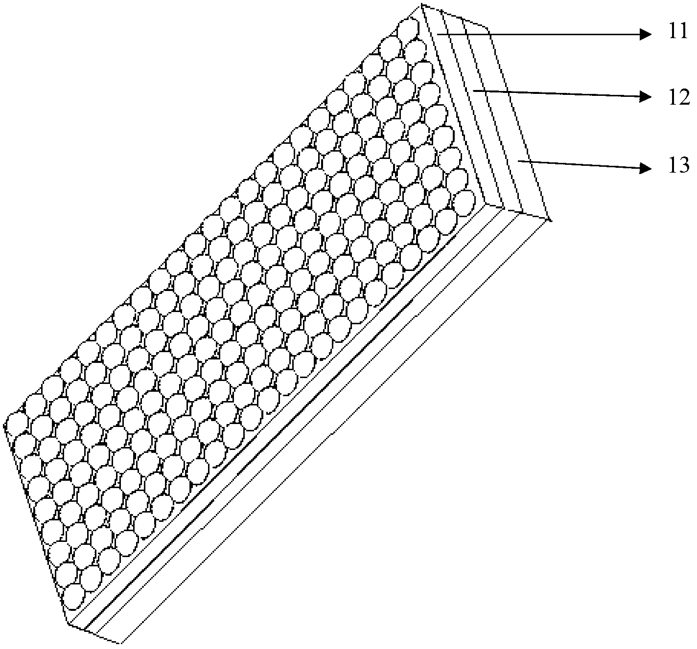
[0057] Such as Figure 1 to Figure 4 As shown, a light reflection plate of the present invention is composed of the first layer 11, the second layer 12 and the third layer 13 sequentially from the outside to the inside, wherein the first layer 11 and the third layer 13 are both composed of The second layer 12 is composed of a material layer of A, and the second layer 12 is composed of a material layer of B, and several hemispherical microstructures are distributed on the surface of the first layer 11 .
[0058] In the foregoing embodiment, the A material layer and the B material layer are composed of the raw material components shown in Table 1;
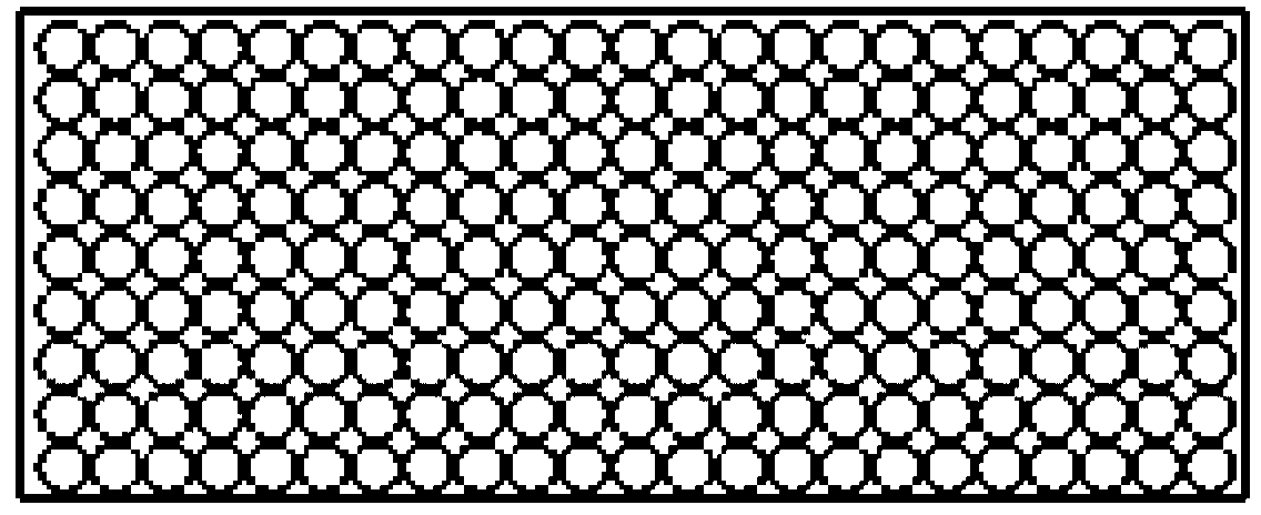
[0059] The diameter of the hemispherical microstructure shown is 15 μm, and the distance between the centers of two adjacent hemispheres is 300 μm, which can also be designed according to actual needs. The preferred characteristic size range for enhancing the reflection effect is 0.1 μm to 1000 μm;
[0060] In the total thickness of...
Embodiment 2
[0082] Such as Figure 9 and Figure 10 As shown, a light reflection plate, its basic structure and performance testing method are the same as in Example 1, and its raw material components and performance testing results are shown in Table 1. The difference is that on the surface of the first layer 11 and the third layer 13 Several hemispherical microstructures are evenly distributed.
[0083] In the above embodiment, the diameter of the shown hemispherical microstructure is 0.1 μm, and the distance between the centers of two adjacent hemispheres is 5 μm; in the total thickness of the light reflection plate, the thickness of the inner layer, that is, the second layer 12, occupies The proportion is 65%, and the proportion of the thickness of the outer layer, that is, the first layer 11 and the third layer 13 is 35%, and the proportion of the thickness of the first layer 11 is 20%.
[0084] Such as Figure 5 to Figure 8 As shown, the specific preparation method of the above-m...
Embodiment 3
[0089] Such as Figure 1 to Figure 4 As shown, a light reflecting plate, its basic structure and performance testing method are the same as in Example 1, and its raw material components and performance testing results are shown in Table 1.
[0090] In the above embodiment, the diameter of the hemispherical microstructure shown is 1000 μm, and the distance between the centers of two adjacent hemispheres is 2500 μm; in the total thickness of the light reflection plate, the proportion of the thickness of the inner layer, that is, the second layer 12 is 90%, the proportion of the thickness of the outer layer, that is, the first layer 11 and the third layer 13 is 10%, and the proportion of the thickness of the first layer 11 is 6%.
[0091] Such as Figure 5 to Figure 8 As shown, the specific preparation method of the above-mentioned light reflection plate of the present invention and the preparation system used are the same as in Example 1, wherein:
[0092] In the step (1), the...
PUM
| Property | Measurement | Unit |
|---|---|---|
| size | aaaaa | aaaaa |
| particle diameter | aaaaa | aaaaa |
| diameter | aaaaa | aaaaa |
Abstract
Description
Claims
Application Information


