Anti-diffusion layer, preparation method of layer, TFT (thin film transistor), array substrate and display device
A technology of thin film transistor and anti-diffusion layer, applied in the fields of anti-diffusion layer and preparation, array substrate, thin film transistor, and display device, can solve the problems of volatilization of low-resistance materials, high ambient temperature, affecting the performance of display device, etc., and achieves simple equipment. , less capital investment, and the effect of improving display quality
- Summary
- Abstract
- Description
- Claims
- Application Information
AI Technical Summary
Problems solved by technology
Method used
Image
Examples
Embodiment 1
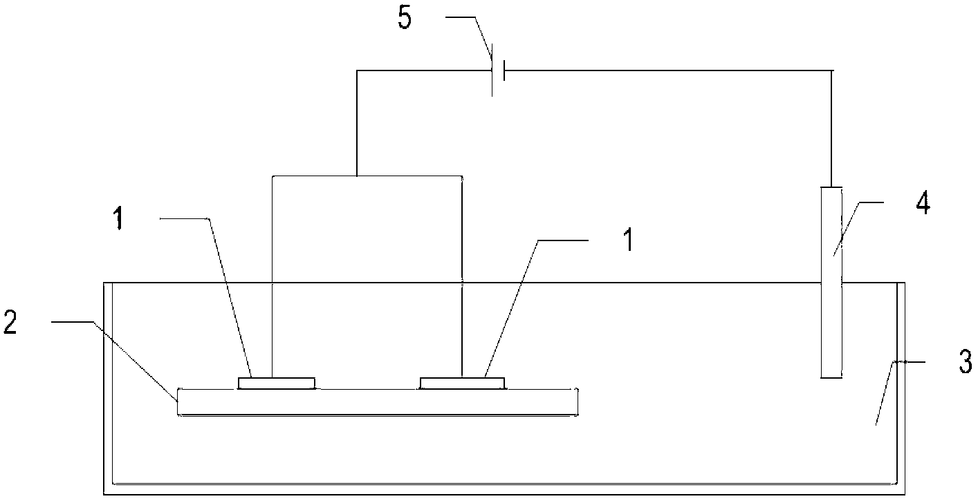
[0016] This embodiment provides a kind of preparation method of anti-diffusion layer, such as figure 1 As shown, it includes: the conductive substrate 1 is used as the anode and placed in the tantalum sulfate solution (that is, the electrolyte 3), and the graphite electrode 4 (other electrodes can also be used, of course) is also placed in the electrolyte 3 as the cathode. An anti-diffusion layer of tantalum dioxide is formed on the conductive substrate 1 by anodic oxidation.
[0017] Wherein, the conductive substrate 1 is preferably a gate of a thin film transistor on the substrate 2, and the material used for the conductive substrate 1 is a low-resistance material. In this embodiment, copper is taken as an example.
[0018] Specifically, the mass concentration range of the tantalum sulfate solution is 6-9%, and the pH value thereof is strictly controlled between 8-10 by using ammonia water, so as to prevent the conductive matrix 1 from being corroded. The AC power supply 5 ...
Embodiment 2
[0025] This embodiment provides an anti-diffusion layer, which is prepared by the method described in Example 1, and the anti-diffusion layer is a tantalum dioxide anti-diffusion layer.
[0026] Since the anti-diffusion layer of this embodiment is prepared by the above-mentioned method, the low-resistance material will not be volatilized during the preparation process, and the performance of the display will not be affected.
Embodiment 3
[0028] This embodiment provides a thin film transistor, which includes a gate disposed above a substrate, and the above-mentioned anti-diffusion layer is formed above the gate; at the same time, a gate insulating layer, a source-drain metal layer, an active layers, passivation layers, and other known structures such as pixel electrodes.
[0029] In the thin film transistor of this embodiment, the gate is preferably made of copper or aluminum.
[0030] Since the above-mentioned anti-diffusion layer is formed on the gate of the thin film transistor of this embodiment, it can effectively prevent copper ions or aluminum ions from diffusing into the gate insulating layer, thereby preventing them from diffusing into the active layer, effectively ensuring Conductivity of thin film transistors.
[0031] The TFT of this embodiment is preferably a bottom-gate type. For a bottom-gate TFT, since the gate is formed prior to the gate insulating layer, the gate can be directly used as a con...
PUM
 Abstract
Description
Claims
Application Information
