Optical system for homogenizing semiconductor laser beam of area array

An optical system and laser beam technology, applied in the field of optical systems, can solve the problems of low energy utilization rate, poor uniformity, and difficult to integrate and assemble, so as to reduce process difficulty and production cost, improve energy utilization rate, and increase the number of divisions. Effect

Inactive Publication Date: 2013-08-14
INST OF OPTICS & ELECTRONICS - CHINESE ACAD OF SCI
View PDF5 Cites 18 Cited by
  • Summary
  • Abstract
  • Description
  • Claims
  • Application Information

AI Technical Summary

Problems solved by technology

The former is not affected by the energy distribution and fluctuations of the incident beam, but the brightness of the beam after homogenization is low, and the system has many components and large volume, which is not easy to integrate and assemble
The latter is mainly composed of a collimator lens, an aspheric microlens array, and a Fourier lens. The system has fewer components, is small in size

Method used


Image

  • Optical system for homogenizing semiconductor laser beam of area array
  • Optical system for homogenizing semiconductor laser beam of area array
  • Optical system for homogenizing semiconductor laser beam of area array

Examples


Embodiment 1

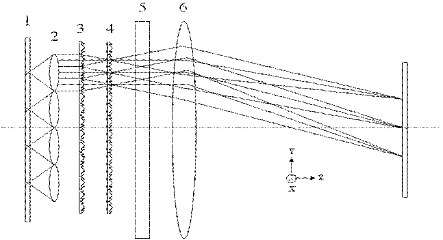
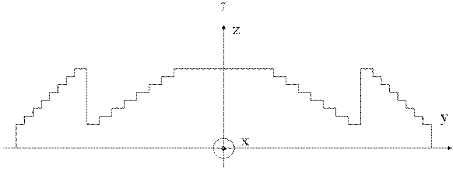
[0036]Using the first microlens array 3 and the second microlens array 4 as the laser homogenizer, the parameters that need to be determined are the parameters of the cylindrical Fresnel diffraction microlens 7 , the slow axis field lens 5 , and the fast axis field lens 6 . The schematic diagram of the area array semiconductor laser beam homogenization system composed of the first microlens array 3 and the second microlens array 4 is as follows: Figure 1a and Figure 1b ,in:

[0037] Parameters of a cylindrical Fresnel diffractive microlens 7: Aperture D FMLA =0.125mm, focal length f FMLA =1.25mm, the number of phase steps N=8;

[0038] Parameters of slow axis field lens 5: focal length f FS =375mm, caliber D FS =127mm, length L FS =160mm;

[0039] Parameters of the fast-axis field lens 6: focal length f FF =300mm, caliber D FF =160mm, length L FF =127mm;

[0040] All materials of the system are silicon dioxide (SILICA).

Embodiment 2

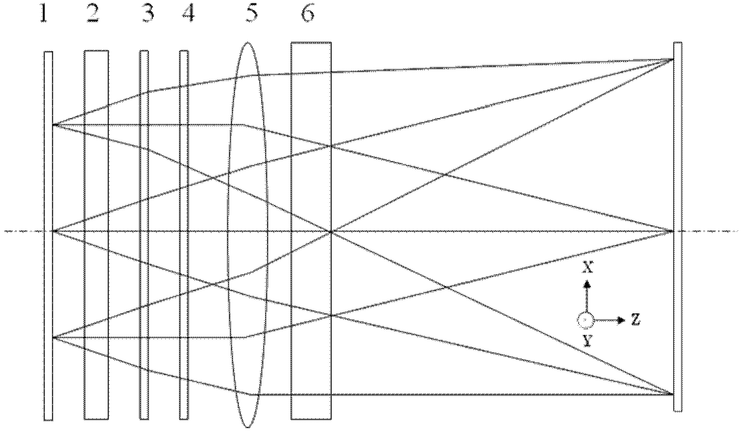
[0042] Using the first microlens array 3 or the second microlens array 4 as a laser homogenizer, the parameters that need to be determined are the parameters of the cylindrical Fresnel diffraction microlens 7 , the slow axis field lens 5 , and the fast axis field lens 6 . The schematic diagram of the area array semiconductor laser beam homogenization system composed of the first microlens array 3 or the second microlens array 4 is as follows: Figure 6a and Figure 6b ,in:

[0043] Parameters of a cylindrical Fresnel diffractive microlens 7: Aperture D FMLA =0.125mm, focal length f FMLA =1.25mm, the number of phase steps N=8;

[0044] Parameters of slow axis field lens 5: focal length f FS =375mm, caliber D FS =127mm, length L FS =160mm;

[0045] Parameters of the fast-axis field lens 6: focal length f FF =300mm, caliber D FF =160mm, length L FF =127mm;

[0046] All materials of the system are silicon dioxide (SILICA).

[0047] In order to verify the feasibility of...


PUM

PropertyMeasurementUnit
Caliberaaaaaaaaaa

Abstract

The invention provides an optical system for homogenizing a semiconductor laser beam of an area array, which comprises a semiconductor laser of the area array, a collimating lens array, a first microlens array, a second microlens array, a slow-axis field lens and a fast-axis field lens, wherein the semiconductor laser of the area array is positioned on the front focal plane of the micro collimating lens array and takes an output laser beam of the semiconductor laser of the area array as a system optical axis; the first microlens array, the second microlens array, the slow-axis field lens and the fast-axis field lens are positioned on the optical axis in sequence and are vertical to the optical axis; and a multi-mode laser beam sent by the semiconductor laser parallelly enters after being collimated by the collimating lens array and then is evenly divided into a plurality of sub beams by the first microlens array to be focused on the rear focal plane, and afterwards, the sub beams are overlaid on the rear focal plane of a field lense by the the second microlens array, the slow-axis field lens and the fast-axis field lens, that is to say, the sub beams are overlaid on the lighting surface. The homogenizing of the semiconductor laser beam is realized by a cylinder-shaped Fresnel diffraction microlens array, so that the quality of the beam is improved.

Description

technical field [0001] The invention relates to the field of laser technology, in particular to an optical system for homogenizing an area array semiconductor laser beam by using an array composed of a plurality of cylindrical Fresnel microlenses. Background technique [0002] Semiconductor lasers are widely used in welding, annealing, cutting, drilling, micro-processing, military, medical and other fields, which have high requirements for the shape, power density, uniformity and stability of the laser beam. Therefore, homogenizing the semiconductor laser beam has become a necessary technical means. [0003] At present, there are two main methods for homogenizing semiconductor laser beams: one is the waveguide method, and the other is the microlens array method. The former is not affected by the energy distribution and fluctuations of the incident beam, but the brightness of the beam after homogenization is low, and the system has many components and is large in size, makin...

Claims


Application Information

Patent Timeline
IPC IPC(8): G02B27/09
Inventor 周崇喜刘志辉杨欢邱传凯
Owner INST OF OPTICS & ELECTRONICS - CHINESE ACAD OF SCI
Why Eureka
Try Eureka