Manufacturing method and special lead frame for lead-out terminal of integrated circuit ceramic packaging shell

A technology of ceramic packaging and integrated circuits, applied in circuits, electrical components, electrical solid devices, etc., can solve problems such as weak strength, unsatisfactory assembly and welding processes, and difficult shape control

Active Publication Date: 2015-09-09
FUJIAN MINHANG ELECTRONICS
View PDF4 Cites 2 Cited by
  • Summary
  • Abstract
  • Description
  • Claims
  • Application Information

AI Technical Summary

Problems solved by technology

[0002] When the pad pitch is 1.27mm, 1.00mm, etc., there is a semi-circular metallized through hole on the periphery of the leadless chip carrier ceramic case (CLCC). When the ceramic case is assembled with the integrated circuit board, the excess solder passes through the half The overflow in the circular metallized through hole forms a meniscus, which can ensure that the excess solder will not affect the electrical performance, and the welding reliability is good; the pad pitch is 0.80mm, 0.60mm, 0.50mm, 0.40mm At the same time, it is difficult to manufacture a semi-circular metallized through hole in the ceramic shell, and it cannot meet the requirements of the assembly and welding process. It is necessary to use a raised pad structure as the lead-out end. The traditional method is to weld metal solder balls on the metal pad. Or blocks form bumps or electroplate on metal pads to form bumps. Each pad is an isolated point. It is difficult and inaccurate to locate isolated points during high-temperature brazing. The mold used for welding is complicated. With the improvement of reliability requirements, such as the need for higher connection strength, adapting to multiple welding assemblies, etc., there are rework times in the structure caused by the use of high-temperature metal solder to form bumps on the metal pads or electroplating to form bumps on the metal pads Restricted, difficult to rework, relatively weak strength and other issues; the formation of bumps by electroplating is costly and difficult to control the shape

Method used


Image

  • Manufacturing method and special lead frame for lead-out terminal of integrated circuit ceramic packaging shell
  • Manufacturing method and special lead frame for lead-out terminal of integrated circuit ceramic packaging shell
  • Manufacturing method and special lead frame for lead-out terminal of integrated circuit ceramic packaging shell

Examples


Embodiment approach

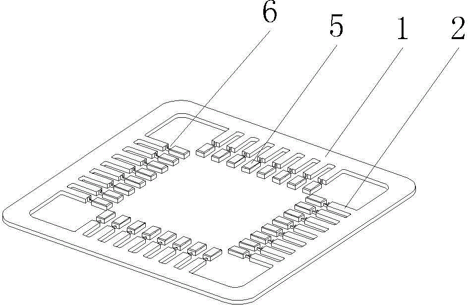
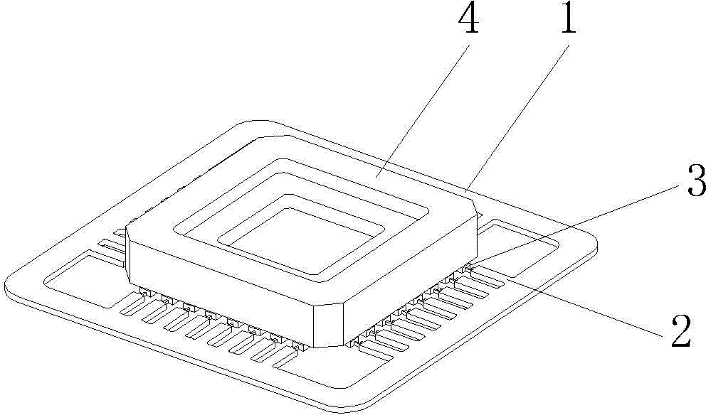
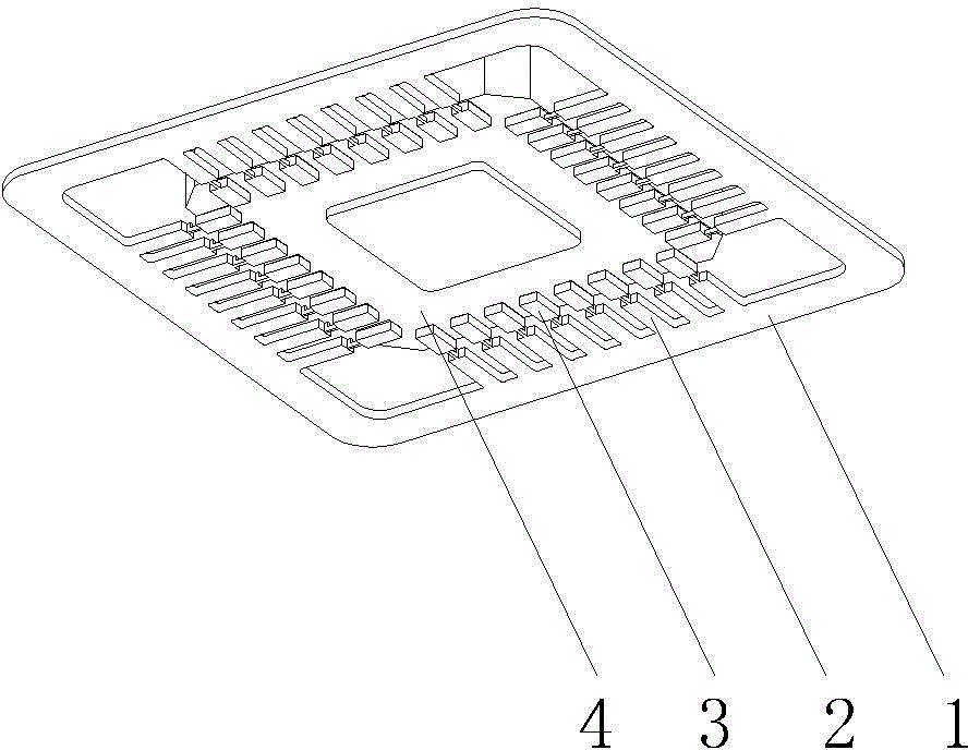
[0019] Figure 5 The first specific implementation of the special lead frame of the method for making the lead end of the integrated circuit ceramic package shell of the present invention is given. It includes the outer frame 1 and the lead 2 to form a grid bar structure with a frame. The lead 2 is Bars, the outer end of the lead 2 is connected to the outer frame 1, the number of the lead 2 is the same as the number of the pads on the ceramic shell 4, the spacing of the lead 2 is the same as that of the pads on the ceramic shell 4, and the inner end of the lead 2 There is a one-to-one correspondence with the pads on the ceramic shell 4 . The material used to make the lead frame can be iron-nickel alloy, kovar, copper sheet or iron-nickel alloy with solder, kovar, copper sheet, etc., and can also be 4J29, 4J42 and other metals. The thickness of the lead frame can be made of 0.1-0.5mm, preferably 0.15-0.25mm in thickness, and the method of making the lead frame can be punching,...


PUM


Abstract

The invention discloses a manufacturing method for leading-out terminals of a ceramic integrated circuit encapsulation casing and a special lead framework. The special lead framework comprises an outer frame 1 and leads 2, and forms a grid bar structure with a frame, wherein the leads 2 are grid bars; the outer ends of the leads 2 are connected with the outer frame, and the inner ends of the leads 2 are in one-to-one correspondence to bonding pads on a ceramic casing 4; after the inner ends of the leads 2 are connected with the bonding pads, the redundant part of the lead framework is cut and separated; and the inner ends of the leads 2 remain on the bonding pads to form bulges so as to form leading-out terminals. Owing to the structure, convenient and accurate positioning is ensured when the leads 2 are welded with the bonding pads, so that a welding die is simplified; and besides, the outer frame can be utilized to achieve direct rack plating, so that the manufacturing technique complexity of the fine-pitch casing is greatly reduced, the production efficiency is improved and the product yield and quality are improved.

Description

technical field [0001] The invention relates to a manufacturing method and a special lead frame for the leading end of an integrated circuit ceramic packaging shell, in particular to a manufacturing method and a special lead frame for the leading end of a fine-pitch non-lead chip carrier ceramic packaging shell, belonging to the technical field of integrated circuit packaging. Background technique [0002] When the pad pitch is 1.27mm, 1.00mm, etc., there is a semi-circular metallized through hole on the periphery of the leadless chip carrier ceramic case (CLCC). When the ceramic case is assembled with the integrated circuit board, the excess solder passes through the half The overflow in the circular metallized through hole forms a meniscus, which can ensure that the excess solder will not affect the electrical performance, and the welding reliability is good; the pad pitch is 0.80mm, 0.60mm, 0.50mm, 0.40mm At the same time, it is difficult to manufacture a semi-circular ...

Claims


Application Information

Patent Timeline
Patent Type & Authority Patents(China)
IPC IPC(8): H01L21/60H01L23/48H01L23/495
CPCH01L2924/0002
Inventor 兰海余咏梅傅建树邹琦
Owner FUJIAN MINHANG ELECTRONICS
Why Eureka
Try Eureka