
Preparation method of P-layer silicon epitaxial wafer on P++ substrate

A technology of silicon epitaxial wafers and substrates, applied in semiconductor/solid-state device manufacturing, electrical components, circuits, etc., can solve problems such as increased leakage current, drastic changes, lattice mismatch, etc., to increase control costs, increase The uniformity of resistivity and the effect of improving the formation of misfit dislocations

Active Publication Date: 2013-08-14
HEBEI POSHING ELECTRONICS TECH
View PDF2 Cites 14 Cited by
  • Summary
  • Abstract
  • Description
  • Claims
  • Application Information

AI Technical Summary

Problems solved by technology

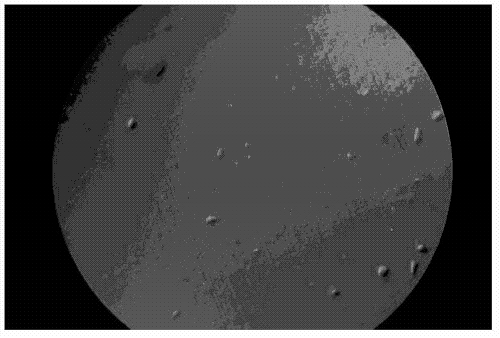
In the device manufacturing process, in order to reduce the voltage drop and energy consumption of the substrate part, some P-type epitaxy uses a heavily boron-doped P++ substrate, and the concentration of boron in the substrate is 3×10 19 ~1×10 20 / cm3, while the epitaxial resistivity is only 5-30 ohm cm, the concentration of B atoms drops sharply during epitaxial growth, the atomic lattice changes drastically, and lattice mismatch occurs. Due to the release of mismatch stress, mismatch dislocations are very large. It is easy to form at the interface of P- / P++ silicon epitaxial wafers, and its accompanying penetrating dislocations that penetrate the entire epitaxial layer will increase the leakage current of the device and cause device failure

Method used


Image

  • Preparation method of P-layer silicon epitaxial wafer on P++ substrate
  • Preparation method of P-layer silicon epitaxial wafer on P++ substrate
  • Preparation method of P-layer silicon epitaxial wafer on P++ substrate

Examples


Embodiment 1

[0041] (1) Use P+ / Boron single-sided polishing sheet, resistivity 0.004~0.0075Ω·cm, thickness 525±15μm, silicon wafer diameter 125±0.2mm, back LTO back seal, edge removal width ≤1mm;

[0042] (2) HCl in-situ polishing is performed at 1100°C, the HCl flow rate is 5slm / 10min, and the removal amount on the surface of the silicon wafer is 0.3 microns;

[0043] (3) Purge: use H 2 Purge the reaction chamber for 8 minutes, and discharge the impurities generated after the surface of the silicon wafer is polished out of the chamber, H 2 The flow rate is 140slm / 10min;

[0044] (4) Double-layer epitaxial growth: using high-purity SiHCl 3 Deposition and growth of resistivity graded layer, growth rate 0.40μm / min, growth temperature 1070°C, resistivity gradient layer thickness 1.4μm; then growth resistivity doped layer, growth temperature 1070°C, growth rate controlled at 0.8μm / min.

Embodiment 2

[0046] (1) Use P+ / Boron single-sided polishing sheet, resistivity 0.004~0.0075Ω·cm, thickness 525±15μm, silicon wafer diameter 125±0.2mm, back LTO back seal, edge removal width ≤1mm;

[0047] (2) HCl in-situ polishing is performed at 1130°C, the HCl flow rate is 5slm / 10min, and the removal amount on the surface of the silicon wafer is 0.4 microns;

[0048] (3) Purge: use H 2 Purge the reaction chamber for 10 minutes, and discharge the impurities generated after the surface of the silicon wafer is polished out of the chamber, H 2 The flow rate is 130slm / 10min;

[0049] (4) Double-layer epitaxial growth: using high-purity SiHCl3 Deposition and growth of the resistivity graded layer, the growth rate is 0.38μm / min, the growth temperature is 1080°C, the thickness of the resistivity gradient layer is 1.5μm; then the resistivity doped layer is grown, the growth temperature is 1100°C, and the growth rate is controlled at 1.0μm / min.

Embodiment 3

[0051] (1) Use P+ / Boron single-sided polished sheet, resistivity 0.004~0.0075Ω·cm, thickness 525±15μm, silicon wafer diameter 125±0.2mm, back LTO back seal, edge removal width ≤1mm;

[0052] (2) HCl in-situ polishing is performed at 1120°C, the HCl flow rate is 5slm / 10min, and the removal amount on the surface of the silicon wafer is 0.3 microns;

[0053] (3) Purge: use H 2 Purge the reaction chamber for 11 minutes, and discharge the impurities generated after the surface of the silicon wafer is polished out of the chamber, H 2 The flow rate is 170slm / 10min;

[0054] (4) Double-layer epitaxial growth: using high-purity SiHCl 3 Deposition and growth of the resistivity gradient layer, the growth rate is 0.42μm / min, the growth temperature is 1100°C, the thickness of the resistivity gradient layer is 1.3μm; then the resistivity doped layer is grown, the growth temperature is 1080°C, and the growth rate is controlled at 0.9μm / min.


PUM

PropertyMeasurementUnit
thicknessaaaaaaaaaa

Abstract

The invention discloses a preparation method of a P-layer silicon epitaxial wafer on a P++ substrate, and belongs to the technical field of silicon epitaxial wafers. The preparation method comprises the steps as follows: (1) selecting a P+<111> / Boron single-face polished section; (2) performing HCl polishing; (3) sweeping; and (4) performing double-layered epitaxial growth: adopting high-purity SiHCl3 deposition, growing a resistivity gradient layer, and then growing a resistivity doped layer. The preparation method adopts a secondary growth process to improve the uniformity of the resistivity of an epitaxial layer; the concentration gradient layer is grown at a low speed, so that formation of misfit dislocation of the epitaxial layer is reduced effectively, the stability and the repeatability of epitaxial electrical properties are improved, and the reliability and the yield of devices are guaranteed.

Description

technical field [0001] The invention relates to the technical field of silicon epitaxial wafers. Background technique [0002] The improvement of the processing capacity of the digital processor has put forward higher requirements for the analog part of the port or analog signal processing. The status of standard MOS in high-speed circuits has been doubted, and various new CMOS process technologies have developed rapidly. Some companies have innovated the original MOS process, among which the use of epitaxial wafers as raw materials to reduce parasitic effects in circuits is one of the most important improvements. Chip speed, integration, power consumption, chip cost, and R&D cycle are important aspects that determine a company's process selection. It is an urgent need to develop qualified epitaxial wafers (mainly P-type materials) for CMOS processes, making standard CMOS processes Development potential in the field of high-speed analog, mixed-signal processing. [0003] C...

Claims


Application Information

Patent Timeline
Patent Type & Authority Applications(China)
IPC IPC(8): H01L21/8238H01L21/8247H01L21/02
Inventor 侯志义袁肇耿薛宏伟赵丽霞田中元许斌武李永辉
Owner HEBEI POSHING ELECTRONICS TECH
Learn More