
Junction-free transverse tunneling field effect transistor

A tunneling field effect, junction-free technology, applied in the direction of semiconductor devices, electrical components, circuits, etc., can solve the problem of limiting the reduction of power supply voltage, and achieve the goal of increasing the switching current ratio, reducing the difficulty of the process, and reducing the size of the device Effect

Active Publication Date: 2013-08-28
TSINGHUA UNIV
View PDF0 Cites 22 Cited by
  • Summary
  • Abstract
  • Description
  • Claims
  • Application Information

AI Technical Summary

Problems solved by technology

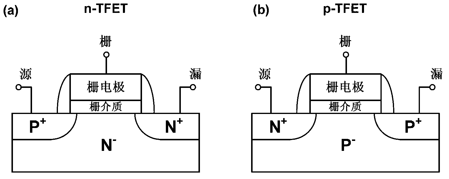
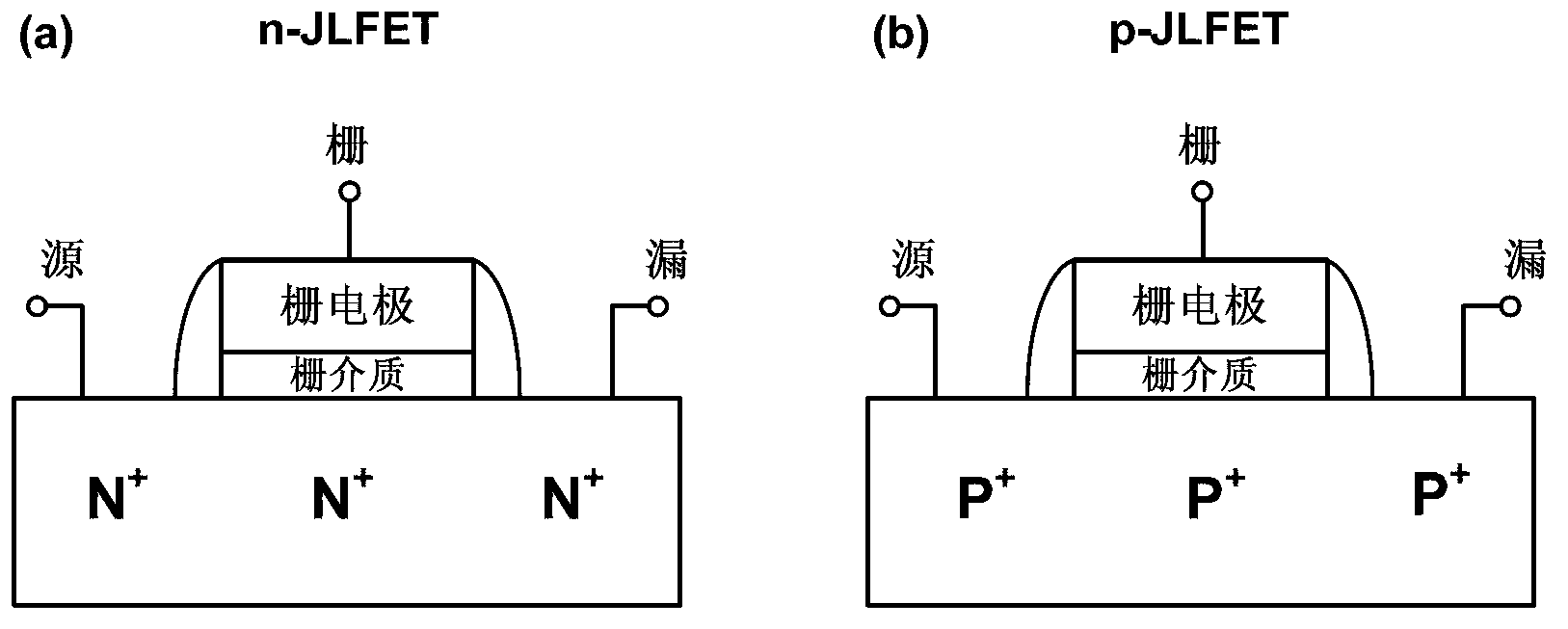
However, with the urgent need for ultra-low power devices, the theoretical limit of the subthreshold slope of the junctionless field effect transistor is still 60mV / decade, which limits the reduction of the power supply voltage.

Method used


Image

  • Junction-free transverse tunneling field effect transistor
  • Junction-free transverse tunneling field effect transistor
  • Junction-free transverse tunneling field effect transistor

Examples


Embodiment Construction

[0025] Embodiments of the present invention are described in detail below, examples of which are shown in the drawings, wherein the same or similar reference numerals designate the same or similar elements or elements having the same or similar functions throughout. The embodiments described below by referring to the figures are exemplary and are intended to explain the present invention and should not be construed as limiting the present invention.

[0026] In describing the present invention, it should be understood that the terms "center", "longitudinal", "transverse", "length", "width", "thickness", "upper", "lower", "front", " Orientation or position indicated by "back", "left", "right", "vertical", "horizontal", "top", "bottom", "inner", "outer", "clockwise", "counterclockwise", etc. The relationship is based on the orientation or positional relationship shown in the drawings, and is only for the convenience of describing the present invention and simplifying the descrip...


PUM


Abstract

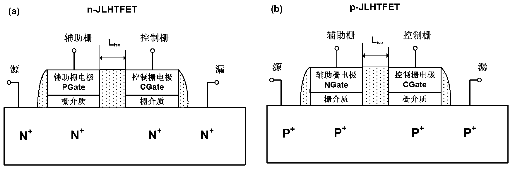
The invention provides a junction-free transverse tunneling field effect transistor which comprises a source region, a drain region, a channel region, a control grid and an auxiliary grid. The source region, the drain region and the channel region form a whole and are made of the same kind of doping type semiconductor materials. The doping density from the source region to a channel and the drain region is the same. The control grid and the auxiliary grid are placed on the same side of the channel, wherein the control grid is used for controlling switch-on and switch-off of a device, and the auxiliary grid is used for enabling transoid to happen to a semiconductor region below the auxiliary grid. The junction-free transverse tunneling field effect transistor is different from a traditional PN junction tunneling field effect transistor. According to the junction-free transverse tunneling field effect transistor, only one doping type is adopted, a PN junction does not need to be manufactured, and technology difficulty is lowered. The junction-free transverse tunneling field effect transistor is beneficial to diminishing the size of the device, restraining a short-channel effect, enlarging the switching current ratio, and improving the subthreshold slope.

Description

technical field [0001] The invention belongs to the technical field of semiconductors, and in particular relates to a junctionless lateral tunneling field effect transistor. Background technique [0002] As we all know, Metal Oxide Semiconductor Field Effect Transistor (MOSFET) is the basic unit of modern electronic components. At present, all transistors have semiconductor junctions, such as PN junctions, heterojunctions, and Schottky junctions. Specifically, the most common homogeneous PN junction is formed by joining a P-type doped region with excess holes and an N-type doped region with excess electrons on the same semiconductor material, heterojunction (Hetero-junction) It is a PN junction composed of two different semiconductor materials, and a Schottky junction is composed of metal and semiconductor contacts. [0003] Typically, a traditional MOSFET device includes a source-channel junction, a drain-channel junction, and a gate stack (including gate dielectric and ga...

Claims


Application Information

Patent Timeline
IPC IPC(8): H01L29/78H01L29/423
Inventor 梁仁荣姚磊王敬许军
Owner TSINGHUA UNIV
Learn More