Ion sensitive sensor and manufacturing method thereof

The technology of an ion-sensitive sensor and a manufacturing method is applied in the field of graphene ion-sensitive sensor based on a field-effect transistor structure and its preparation field, which can solve problems such as difficult industrial production, few detection samples, and poor selectivity, and achieve short response time, The effect of convenient operation and low cost

Active Publication Date: 2013-09-11
SUZHOU INST OF NANO TECH & NANO BIONICS CHINESE ACEDEMY OF SCI
View PDF1 Cites 44 Cited by
  • Summary
  • Abstract
  • Description
  • Claims
  • Application Information

AI Technical Summary

Problems solved by technology

[0004] Although a lot of exploration has been made in the research of ion-sensitive sensors based on graphene transistors, and there are simple sensor samples, but at present, many io...

Method used


Image

  • Ion sensitive sensor and manufacturing method thereof
  • Ion sensitive sensor and manufacturing method thereof
  • Ion sensitive sensor and manufacturing method thereof

Examples


Embodiment 1

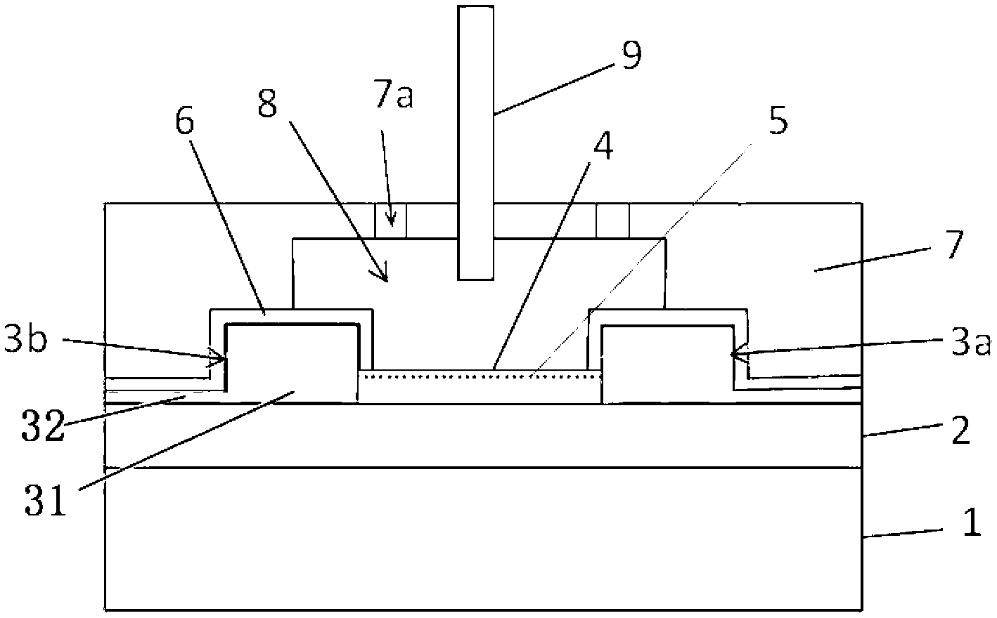
[0037] Such as figure 1 Shown, the graphene ion sensitive sensor of the present embodiment comprises:

[0038] stacking silicon oxide layer 2 and silicon substrate 1 up and down;

[0039] The source electrode 3a and the drain electrode 3b arranged on the silicon oxide layer 2 at intervals; the source electrode 3a and the drain electrode 3b each include a plug-in portion 31 and a socket for electrical connection with an external circuit (not shown in the figure). extension 32;

[0040] The graphene layer 4 arranged on the surface of the silicon oxide layer 2 between the source electrode 3a and the drain electrode 3b, the graphene layer 4 is respectively connected to the source electrode 3a inserting portion 31 and the drain electrode 3b inserting portion 31 connection; the surface layer of the graphene layer 4 is permeated with metal oxide particles 5;

[0041] An insulating layer 6 covering the surfaces of the source electrode 3a and the drain electrode 3b.

[0042] The mi...

Embodiment 2

[0067] The structure of the graphene ion-sensitive sensor of this embodiment is the same as that of Embodiment 1. The difference is that the source and drain are made of Pt, and the insulating layer is made of photoresist AZ4602.

[0068] Moreover, in this embodiment, a graphene solution with a concentration of 0.1 mg / mL is printed between the source electrode and the drain electrode by an aerosol printing method. Then place the chip in 1mol / L NiCl 2 , 0.2mol / L NH 4 Cl and 0.06875mol / L NaOH mixed solution, placed in a constant temperature oven at 55°C for 40min. Then place the chip under the protection of Ar gas for annealing at 350° C. for 120 minutes, and keep it warm for 2 hours.

[0069] The remaining steps can be shown in Example 1 with reference to.

Embodiment 3

[0071] The structure of the graphene ion-sensitive sensor of this embodiment is the same as that of Embodiment 1. The difference is that the source and drain are made of Pt, and the insulating layer is made of polymethyl methacrylate.

[0072] Moreover, in this embodiment, a graphene solution with a concentration of 0.05 mg / mL is printed between the source electrode and the drain electrode by means of aerosol printing. Then place the chip in 1mol / L NiCl 2 , 0.2mol / L NH 4 Cl and 0.06875mol / L NaOH mixed solution, placed in a constant temperature oven at 55°C for 30min. Then place the chip under the protection of Ar gas for annealing at 350° C. for 30 minutes, and keep it warm for 2 hours.

[0073] The remaining steps can be shown in Example 1 with reference to.


PUM

PropertyMeasurementUnit
Concentrationaaaaaaaaaa
Resistanceaaaaaaaaaa
Diameteraaaaaaaaaa

Abstract

The invention relates to an ion sensitive sensor comprising a silicon oxide layer and a silicon substrate which are vertically stacked, a source electrode and a drain electrode arranged on the silicon oxide layer at an interval, and a graphene layer arranged on the surface of the silicon oxide layer and between the source electrode and the drain electrode; wherein the graphene layer is respectively connected with a gear shaping part of the source electrode and a gear shaping part of the drain electrode, and the surface layer of the graphene layer is penetrated with metal oxide particles; the ion sensitive sensor also comprises a micro fluidic channel layer which is erected on the gear shaping part of the source electrode and the gear shaping part of the drain electrode, and the gear shaping part of the source electrode and the gear shaping part of the drain electrode are coated with insulating layers; the micro fluidic channel layer is matched with the graphene layer to form a cavity for accommodating an object for measurement, and is opened with through holes; and suspended grid electrodes are inserted into the through holes and extend into the cavity. The ion sensitive sensor has a structure which is similar to a field effect transistor, and has advantages of high flux, high sensitivity, short response time and the like.

Description

technical field [0001] The invention relates to the technical field of sensors, in particular to a graphene ion-sensitive sensor based on a field-effect transistor structure and a preparation method thereof. Background technique [0002] At present, the endless environmental pollution incidents have attracted more and more public attention, and the society has put forward higher requirements for the real-time, sensitivity and selectivity of monitoring pollutants (sewage, waste gas, solid waste). Traditional environmental monitoring usually adopts off-line and laboratory analysis methods, which have slow analysis speed, complicated operation, large and expensive analytical instruments, and cannot perform on-site rapid analysis and continuous online monitoring. Therefore, as a new means of obtaining detection information, sensor technology has been widely used in the field of environmental monitoring due to its advantages of low cost, easy portability, and high selection sensi...

Claims


Application Information

Patent Timeline
IPC IPC(8): G01N27/414
Inventor 张珽于薇李光辉刘瑞沈方平其他发明人请求不公开姓名
Owner SUZHOU INST OF NANO TECH & NANO BIONICS CHINESE ACEDEMY OF SCI
Why Eureka
Try Eureka