Nanometer semi-conductive non-woven fabric and processing technology thereof

A processing technology and non-woven fabric technology, applied in the field of nano-semiconductive non-woven fabrics and its processing technology, can solve the problems of low tensile strength, easy to fall off, large surface resistance, large volume resistance, etc., to achieve high tensile strength, Small volume resistance, environment-friendly effect

Inactive Publication Date: 2013-09-11
YANG ZHOU TENGFEI ELECTRIC CABLE & APPLIANCE MATERIALS CO LTD
View PDF6 Cites 7 Cited by
  • Summary
  • Abstract
  • Description
  • Claims
  • Application Information

AI Technical Summary

Problems solved by technology

The disadvantage is that the inside of the fiber itself is not conductive, and it only relies on the "C" black component on the surface to conduct electricity after dipping.

Method used


Image

  • Nanometer semi-conductive non-woven fabric and processing technology thereof
  • Nanometer semi-conductive non-woven fabric and processing technology thereof
  • Nanometer semi-conductive non-woven fabric and processing technology thereof

Examples


Embodiment 1

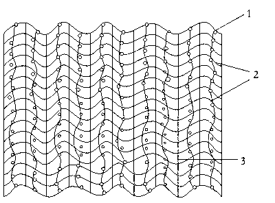
[0023] The invention comprises a fiber net formed by interweaving conductive carbon fiber short fibers 2; the fiber net is longitudinally and parallelly arranged with reinforcing carbon fiber polyester yarns 3; the surface of the fiber net is coated with conductive liquid.

[0024] The fiber web: the grammage is 10g / ㎡.

[0025] The reinforced carbon fiber polyester yarn 3: the thickness is 30dtex, and the distance between the yarns is between 2mm.

[0026] Nano-semiconductive non-woven fabric processing technology, according to the following process steps:

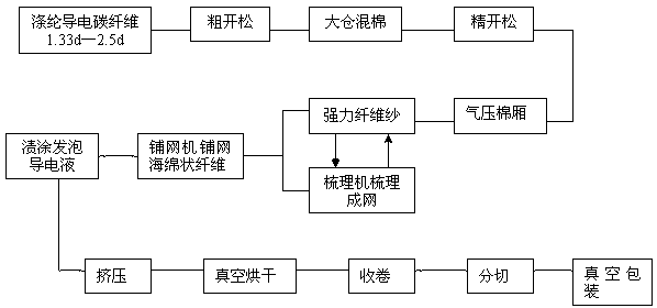
[0027] 1) Using new conductive carbon fiber staple fiber 2 new materials: After non-woven fabric carding process: fiber staple fiber 2 rough opening → big warehouse blending → fine opening → air pressure cotton box → carding machine → web laminating machine, forming A layer of fiber sponge with a uniform thickness, the weight is 10g / ㎡;

[0028] 2) Longitudinal linear laying process of high-strength yarn: the reinforced c...

Embodiment 2

[0038] The invention comprises a fiber net formed by interweaving conductive carbon fiber short fibers 2; the fiber net is longitudinally and parallelly arranged with reinforcing carbon fiber polyester yarns 3; the surface of the fiber net is coated with conductive liquid.

[0039] The fiber web: the grammage is 70g / ㎡.

[0040] The reinforced carbon fiber polyester yarn 3: the thickness is 50dtex, and the distance between the yarns is between 5mm.

[0041] Nano-semiconductive non-woven fabric processing technology, according to the following process steps:

[0042] 1) Using new conductive carbon fiber staple fiber 2 new materials: After non-woven fabric carding process: fiber staple fiber 2 rough opening → big warehouse blending → fine opening → air pressure cotton box → carding machine → web laminating machine, forming A layer of fiber sponge with a uniform thickness, the weight is 70g / ㎡;

[0043] 2) Longitudinal linear laying process of high-strength yarn: the reinforced c...

Embodiment 3

[0053] The invention comprises a fiber net formed by interweaving conductive carbon fiber short fibers 2; the fiber net is longitudinally and parallelly arranged with reinforcing carbon fiber polyester yarns 3; the surface of the fiber net is coated with conductive liquid.

[0054] The fiber web: the grammage is 50g / ㎡.

[0055] The reinforced carbon fiber polyester yarn 3: the thickness is 40dtex, and the distance between the yarns is between 3mm.

[0056] Nano-semiconductive non-woven fabric processing technology, according to the following process steps:

[0057] 1) Using new conductive carbon fiber staple fiber 2 new materials: After non-woven fabric carding process: fiber staple fiber 2 rough opening → big warehouse blending → fine opening → air pressure cotton box → carding machine → web laminating machine, forming A layer of fiber sponge with uniform thickness, the weight is 50g / ㎡;

[0058] 2) Longitudinal linear laying process of high-strength yarn: the reinforced car...


PUM


Abstract

The invention relates to a nanometer semi-conductive non-woven fabric and a processing technology of the nanometer semi-conductive non-woven fabric. The nanometer semi-conductive non-woven fabric is made of carbon fiber new materials through the advanced technologies like the high-strength spun yarn assisted net new process, the nanometer technology, the foam terylene layer technology and vacuum drying. The nanometer semi-conducive non-woven fabric has the advantages of being superior in semi-conductive performance, high in anti-tension strength, low in surface resistance and volume resistance and not prone to fading under high temperature. Besides, 'C' black on the surface cannot drop, efficiency is high, energy is saved, and environmental friendliness is achieved in a manufacturing process. The nanometer semi-conductive non-woven fabric is mainly used in cable core insulating layers of mine cables with 6KV and more than 6KV high voltage, shipboard cables with 6KV and more than 6KV high voltage and large-cross-section power cables with 10KV or more than 10KV and copper conductor surface taped coverings, capable of resisting strong electric fields and static, and semi-shielding. The nanometer semi-conductive non-woven fabric is also applicable to the development of indoor anti-static devices and anti-radiation shielding layers of medical and maternity anti-radiation clothes.

Description

technical field [0001] The invention relates to a nano-semiconductive non-woven fabric and a processing technology thereof, belonging to cable wrapping materials. Background technique [0002] At present, the production of semi-conductive non-woven fabrics at home and abroad is made by impregnating polyester fibers in conductive liquid and drying them. The disadvantage is that the inside of the fiber itself is not conductive, and it only relies on the "C" black component on the surface to conduct electricity after dipping. . Contents of the invention [0003] In view of the above defects, the present invention aims to provide a nano-semiconductive non-woven fabric and its processing technology. [0004] For this reason, the technical solution adopted by the present invention is: the present invention comprises a fiber web formed by interweaving conductive carbon fiber short fibers; the fiber web is longitudinally parallel with reinforced carbon fiber polyester yarn; the...

Claims


Application Information

Patent Timeline
Patent Type & Authority Applications(China)
IPC IPC(8): H01B17/64H01B3/02B32B19/06B32B33/00
Inventor 张云张玉梅杨正龙周敏玉
Owner YANG ZHOU TENGFEI ELECTRIC CABLE & APPLIANCE MATERIALS CO LTD
Why Eureka
Try Eureka