

Metallic oxide thin film transistor and manufacturing method thereof
An oxide thin film and oxide semiconductor technology, applied in transistors, semiconductor/solid-state device manufacturing, electrical components, etc., can solve problems such as increasing cost and difficulty of preparation process, reducing device aperture ratio, and affecting the performance of metal oxide semiconductors. , to achieve better display effect, large source-drain current, and improved carrier mobility.
- Summary
- Abstract
- Description
- Claims
- Application Information
AI Technical Summary
Problems solved by technology
Method used
Image

Examples
Embodiment 1
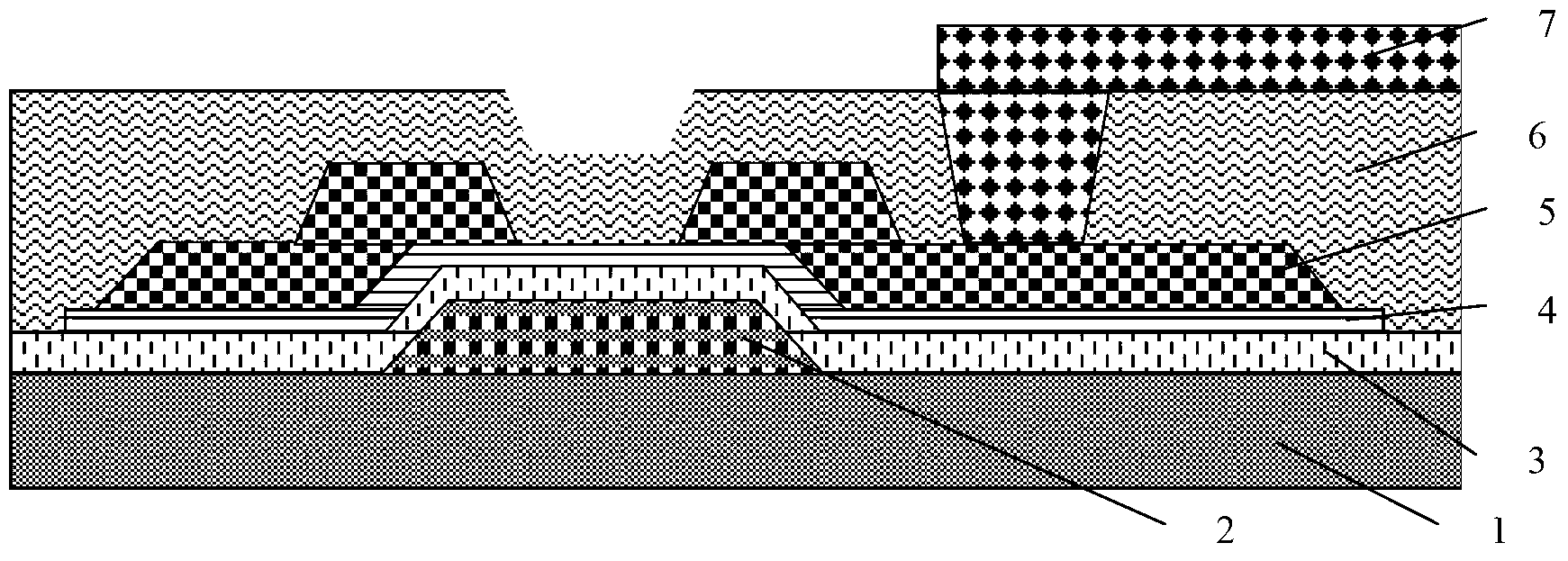
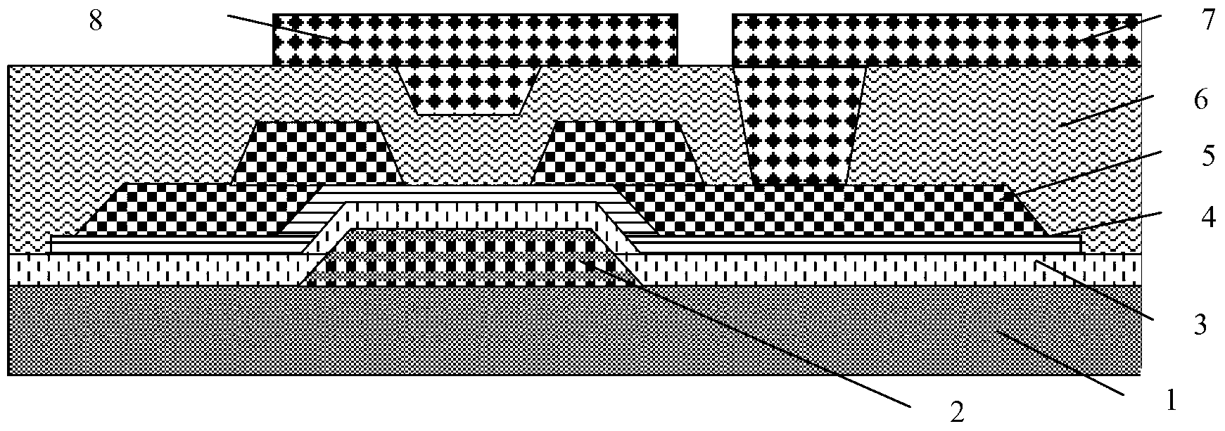
[0054] This embodiment provides a metal oxide thin film transistor, such as figure 2 As shown, it includes a substrate 1, and a gate 2, a gate insulating layer 3, a metal semiconductor oxide layer 4, a source / drain conductive layer 5, and an interlayer insulating layer 6 arranged in sequence along a direction away from the substrate 1, The interlayer insulating layer 6 fills the gap between the source conductive layer and the drain conductive layer to form a channel layer; an anode conductive layer 7 and a conductive upper gate 8 are formed on the upper surface of the interlayer insulating layer 6; The upper gate 8 completely covers the channel layer, and the light reflectance of its material is greater than 85%.
[0055] This embodiment also provides a method for preparing the above-mentioned metal oxide thin film transistor, such as Figure 3A to Figure 3F shown, including the following steps:
[0056] S1. On the substrate 1, the gate 2, the gate insulating layer 3, the m...
Embodiment 2
[0068] In this embodiment, as a further improvement of Embodiment 1, the work function of the material of the upper grid 8 is between 4.9ev-5.2ev; more preferably, the surface resistance of the material of the upper grid 8 is less than 10Ω / □.
[0069] In the prior art, there are many materials that meet the above conditions. Considering the relatively mature materials used in OLED devices, the material of the upper gate 8 includes any one of the following groups of materials: ITO / Ag / ITO, ITO / Ag, ITO / Al / ITO, ITO / Al. The above materials are only preferred embodiments of this application, and other qualified materials can also be selected.
Embodiment 3
[0071] In order to make the manufacturing process of the metal oxide semiconductor thin film transistor simpler, the anode conductive layer 7 is made of the same material as the upper gate 8 .
[0072] In the method for preparing the metal oxide thin film transistor, the step S2 also includes the following steps:
[0073] S2_1. Photoetching an anode contact hole pattern on the interlayer insulating layer 6, and etching to obtain an anode contact hole, the anode contact hole penetrates the interlayer insulating layer 6 and communicates with the metal oxide semiconductor layer 4;
[0074] S2_2. Deposit a layer of anode conductive material on the interlayer insulating layer 6, the anode conductive material fills the anode contact hole and contacts the metal oxide semiconductor layer 4; the method for depositing the anode conductive material includes: Physical vapor deposition method, evaporation method and other deposition methods, etc.;
[0075] S2_3, photoetching an upper grid...
PUM
| Property | Measurement | Unit |
|---|---|---|
| electron work function | aaaaa | aaaaa |
| reflectance | aaaaa | aaaaa |
Abstract
Description
Claims
Application Information