Biodegradable flexible conductive base plate and preparation method thereof

A flexible conductive and rigid substrate technology, applied in semiconductor/solid-state device manufacturing, circuits, electrical components, etc., can solve the problems of environmental and biological hazards, high price, heavy weight, etc., to reduce solid pollution, simple preparation process, high flatness effect

Inactive Publication Date: 2013-09-18
UNIV OF ELECTRONIC SCI & TECH OF CHINA
View PDF3 Cites 32 Cited by
  • Summary
  • Abstract
  • Description
  • Claims
  • Application Information

AI Technical Summary

Problems solved by technology

In addition to being expensive, quartz substrates and silicon substrates have the same disadvantages as glass substrates, such as fragile, relatively heavy, inconvenient to carry, and non-degradable; although plastic subst

Method used


Image

  • Biodegradable flexible conductive base plate and preparation method thereof

Examples


Embodiment 1

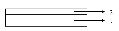
[0031] Such as figure 1 As shown, the biodegradable flexible substrate 1 of the substrate is silk fibroin, the conductive layer 2 is carbon nanotubes, and the thickness of the conductive layer is 200 nm. The entire device structure is described as:

[0032] Silk Fibroin / Carbon Nanotubes

[0033] The preparation method is as follows:

[0034] ① Use acetone, ethanol solution and deionized water to ultrasonically clean the surface of the glass substrate with a surface roughness less than 1 nm, and dry it with dry nitrogen after cleaning.

[0035] ② Prepare the conductive layer of carbon nanotubes by spin-coating, the spin-coating speed is 1000 rpm, the duration is 30s, the film thickness is 200 nm, and then the substrate is thermally annealed at 130°C;

[0036] ③The silk fibroin solution with a concentration of 10 wt% was drip-coated on the glass substrate, and the substrate was heated to 60°C to dry the solution.

[0037] ④ Peel off the dried biodegradable flexible conductiv...

Embodiment 2

[0040] Such as figure 1 As shown, the substrate is a biodegradable flexible substrate 1 viral cellulose, the conductive layer is silver nanowires, and the thickness of the conductive layer is 180 nm. The entire device structure is described as:

[0041] Viral Cellulose / Silver Nanowires

[0042] The preparation process is similar to Example 1.

Embodiment 3

[0044] Such as figure 1 As shown, the biodegradable flexible substrate 1 of the substrate is gelatin, the conductive layer 2 is gold nanowires, and the thickness of the conductive layer is 160 nm. The entire device structure is described as:

[0045] Gelatin / gold nanowires

[0046] The preparation process is similar to Example 1.


PUM

PropertyMeasurementUnit
Thicknessaaaaaaaaaa
Thicknessaaaaaaaaaa
Surface roughnessaaaaaaaaaa

Abstract

The invention discloses a biodegradable flexible conductive base plate and a preparation method thereof. The base plate comprises a biodegradable flexible substrate and a conductive layer, wherein the flexible substrate is made from a biodegradable material; the conductive layer is attached to the surface of the biodegradable flexible substrate. The base plate disclosed by the invention has not only conductive capability but also biodegradable property and can be widely applied to preparation of a flexible photo-electronic/electronic device; an application range of the photo-electronic/electronic device is widened and the environmental pollution caused by electronic wastes can also be reduced.

Description

technical field [0001] The invention relates to the fields of organic optoelectronic / electronic technology, biology and environmental science, in particular to a biodegradable flexible conductive substrate and a preparation method thereof. Background technique [0002] Organic optoelectronics / electronics technology is a rapidly developing industry with high technological content after microelectronics technology. With the rapid development of organic optoelectronic / electronic technology, optoelectronic / electronic products such as organic solar cells, sensors, and thin film transistors have gradually matured, and they have greatly improved people's lives. At the same time, the wide application of optoelectronic / electronic technology in various fields of social life has also created a huge growing market. However, with the increasing development of technology, many problems have also been brought. Firstly, conventional rigid substrates used in optoelectronic / electronic devic...

Claims


Application Information

Patent Timeline
IPC IPC(8): B32B5/00B32B33/00H01L23/14H01L21/48
Inventor 于军胜李海强郑毅帆张磊
Owner UNIV OF ELECTRONIC SCI & TECH OF CHINA
Why Eureka
Try Eureka