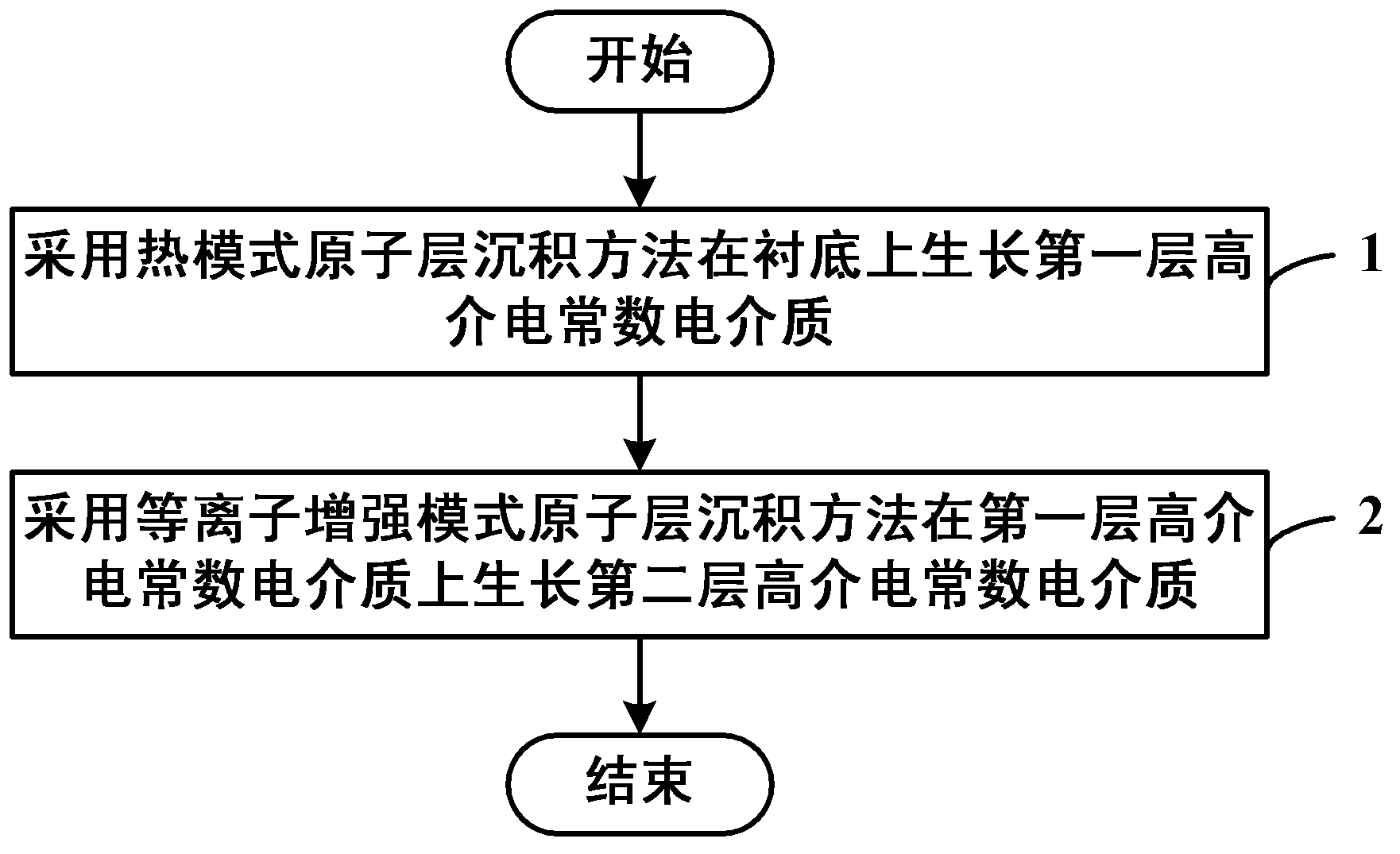
Method for growing high-dielectric constant dielectric lamination
A high dielectric constant, dielectric technology, used in circuits, electrical components, semiconductor/solid-state device manufacturing, etc., to avoid electrical performance degradation, avoid ion damage and interface oxidation, and accurately control the film thickness.
- Summary
- Abstract
- Description
- Claims
- Application Information
AI Technical Summary
Problems solved by technology
Method used
Image


Examples
Embodiment 1
[0041] A preferred embodiment of the present invention applied to a MOS process with a micron-level gate length will be described in detail below with reference to the accompanying drawings.
[0042] Step 1) Clean the substrate:
[0043] Rinse the GaAs substrate with MOS-grade acetone for 5 minutes, and apply ultrasound in a water bath with a power of 15W;
[0044] Rinse with MOS-grade ethanol for 5 minutes, and then apply ultrasound with a power of 15W in a water bath;
[0045] Rinse with deionized water for 3 minutes and blow dry with high-purity nitrogen;
[0046] Soak the GaAs substrate with hydrochloric acid and deionized water with a volume ratio of 1:10 for 1 minute;
[0047] Soak in MOS-grade ammonia water for 5 minutes;
[0048] Rinse with deionized water for 3 minutes and blow dry with high-purity nitrogen.
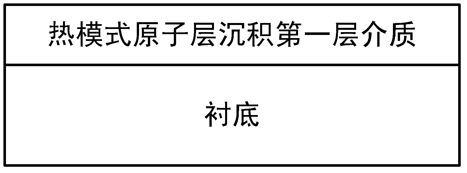
[0049] like figure 2 shown.
[0050] Step 2) Thermal Mode Atomic Layer Deposition of Aluminum Oxide:
[0051] The GaAs substrate cleaned in step 1) is p...
Embodiment 2
[0072] An embodiment of the present invention applied to a MOS process with a micron-scale gate length will be described in detail below with reference to the accompanying drawings.
[0073] Step 1) Clean the substrate:
[0074] Rinse the GaAs substrate with MOS-grade acetone for 5 minutes, and apply ultrasound in a water bath with a power of 15W;
[0075] Rinse with MOS-grade ethanol for 5 minutes, and then apply ultrasound with a power of 15W in a water bath;
[0076] Rinse with deionized water for 3 minutes and blow dry with high-purity nitrogen;
[0077] Soak the GaAs substrate with hydrochloric acid and deionized water with a volume ratio of 1:10 for 1 minute;
[0078] Soak in MOS-grade ammonia water for 5 minutes;
[0079] Rinse with deionized water for 3 minutes and blow dry with high-purity nitrogen.
[0080] like figure 2 shown.
[0081] Step 2) Thermal Mode ALD Oxide:
[0082] Here thermal mode atomic layer deposition of 0A oxide was carried out directly to s...
PUM
| Property | Measurement | Unit |
|---|---|---|
| Thickness | aaaaa | aaaaa |
Abstract
Description
Claims
Application Information
 - R&D
- Intellectual Property
- Life Sciences
- Materials
- Tech Scout
- Unparalleled Data Quality
- Higher Quality Content
- 60% Fewer Hallucinations
Browse by: Latest US Patents, China's latest patents, Technical Efficacy Thesaurus, Application Domain, Technology Topic, Popular Technical Reports.
© 2025 PatSnap. All rights reserved.Legal|Privacy policy|Modern Slavery Act Transparency Statement|Sitemap|About US| Contact US: help@patsnap.com