
Manufacturing method for metal connected wire and manufacturing method for semiconductor structure

A manufacturing method and metal wiring technology, applied in the manufacture of semiconductor/solid-state devices, electrical components, circuits, etc., can solve the problems of uneven metal growth rate, affecting the electrical performance and reliability of metal wiring, and achieve hole defects. The effect of reducing and optimizing the strength of the film layer

Active Publication Date: 2015-04-29
SEMICON MFG INT (SHANGHAI) CORP
View PDF5 Cites 0 Cited by
  • Summary
  • Abstract
  • Description
  • Claims
  • Application Information

AI Technical Summary

Problems solved by technology

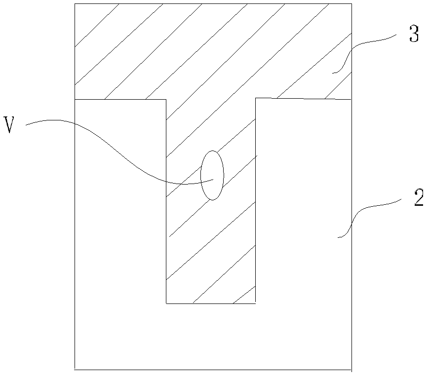
However, during the process of filling the metal material, due to the uneven growth rate of the metal at different positions on the upper and lower parts of the trench, it often leads to the generation of hole defects V in the trench, such as figure 1 shown
The existence of holes seriously affects the electrical performance and reliability of metal wiring

Method used


Image

  • Manufacturing method for metal connected wire and manufacturing method for semiconductor structure
  • Manufacturing method for metal connected wire and manufacturing method for semiconductor structure
  • Manufacturing method for metal connected wire and manufacturing method for semiconductor structure

Examples


no. 1 example

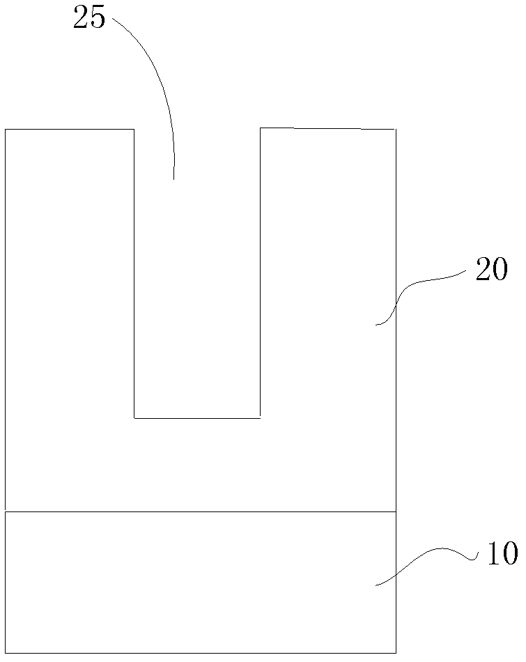
[0060] First, if image 3 , providing a semiconductor substrate 10 . The semiconductor substrate 10 may be a common bulk silicon substrate, or a silicon-on-insulator (SOI) substrate, or a substrate of other materials than silicon. In addition, semiconductor structures, such as transistor gates, capacitors, or interlayer metal layers, may have been formed on the substrate.

[0061] continue to participate image 3 , depositing a dielectric layer 20 on the semiconductor substrate 10 , and then forming a trench 25 in the dielectric layer 20 . As an example, the material of the dielectric layer 20 may be silicon oxide, and its formation method may be a common chemical vapor deposition process. In other embodiments, the dielectric layer 20 may be other low-K dielectric materials, such as compounds formed by Si, O, C, etc., such as silicon oxide.

[0062] Then, the metal material 30 is filled in the groove 25 , and the metal material 30 at least fills the groove 25 . Due to pro...

no. 2 example

[0073] Although in the process of electromagnetic radiation, the heating degree of the dielectric layer is much smaller than that of the metal layer, in some cases, such as the selection of the electromagnetic spectrum or electromagnetic intensity, it is impossible to satisfy the heating of the metal material and the heating of the dielectric layer at the same time. The amount is small enough to damage the dielectric layer as a last resort; or due to some unavoidable reasons, such as the contact between the dielectric layer and the metal material may be damaged by the heat transfer of the metal material. The second embodiment involves the removal of the aforementioned damage. The following is a detailed description of the second embodiment.

[0074] Firstly, a dielectric layer, trenches, metal materials, etc. are formed using the same or substantially the same process as the first embodiment, and electromagnetic radiation treatment is performed on the metal materials. formed ...

no. 3 example

[0078] Different from the method of grinding and removing the damaged dielectric layer in the second embodiment, the third embodiment provides another method for repairing the damaged dielectric layer, and the method does not cause loss of conductive materials. The following is a detailed description of the third embodiment.

[0079] Firstly, the dielectric layer 20, the trench 25, the metal material 30, etc. are formed by the same or substantially the same process as the first embodiment, and the metal material 30 is subjected to electromagnetic radiation treatment. formed structure with Figure 5 Much the same.

[0080] Then, a chemical mechanical polishing (CMP) process is performed with the dielectric layer 20 as a stop layer to remove the metal material 30 above the dielectric layer 20 . formed structure with Image 6 Much the same.

[0081] Next, if Figure 7 , all the dielectric layers 20 on both sides of the conductive material 30 are removed, and spaces 40 are fo...


PUM


Abstract

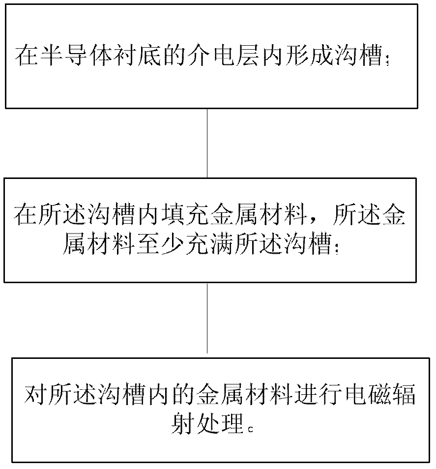
The invention provides a manufacturing method for a metal connected wire and a manufacturing method for a semiconductor structure. The manufacturing method for the metal connected wire comprises the following steps of forming a trough in a dielectric layer of a semiconductor substrate; filling a metal material in the trough, wherein the trough is at least fully filled with the metal material; and carrying out electromagnetic radiation processing on the metal material in the trough. The semiconductor metal material has strong absorbing capacity for electromagnetic radiation such as infrared light and microwave, so that after the semiconductor metal material is radiated, the metal material in the trough can generate a great deal of heat and is fused for eliminating the cavity defect in the trough.

Description

technical field [0001] The invention relates to a manufacturing process of a semiconductor device, in particular to a manufacturing method of a metal connection structure. Background technique [0002] Metal wiring is the most basic interconnection structure in the semiconductor manufacturing process. Regardless of the dual damascene process or the general manufacturing process, the manufacturing process of the metal connection usually includes the steps of forming a trench (not shown) in the dielectric layer 2 and filling the trench with a metal material 3 . However, during the process of filling the metal material, due to the uneven growth rate of the metal at different positions on the upper and lower parts of the trench, it often leads to the generation of hole defects V in the trench, such as figure 1 shown. The existence of holes seriously affects the electrical performance and reliability of metal wiring. [0003] Therefore, it is necessary to improve the prior art...

Claims


Application Information

Patent Timeline
Patent Type & Authority Patents(China)
IPC IPC(8): H01L21/768
Inventor 王冬江张海洋徐依协
Owner SEMICON MFG INT (SHANGHAI) CORP
Learn More