Integrated LED light-emitting device and manufacturing method thereof
A technology of light-emitting devices and manufacturing methods, which is applied in semiconductor/solid-state device manufacturing, semiconductor devices, electric solid-state devices, etc., can solve problems such as poor connection stability, achieve better heat dissipation effects, better heat dissipation, and facilitate batch use Effect
- Summary
- Abstract
- Description
- Claims
- Application Information
AI Technical Summary
Problems solved by technology
Method used
Image
Examples
Embodiment 1
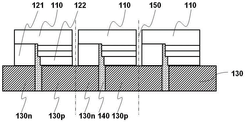
[0042]In this embodiment, in order to simplify the drawings and facilitate description, three LED light-emitting units are used to form an integrated LED light-emitting device. number.
[0043] Please see attached figure 1 , an integrated LED light-emitting device, including: a light-emitting epitaxial unit 110 , ohmic contact layers 121 , 122 , an electrode pad layer 130 , and an insulator 140 . Specifically, the epitaxial layers of each light-emitting epitaxial unit 110 are isolated from each other through the isolation channel 150 , and in a preferred embodiment, the isolation channel 150 can be filled with an insulating material. The light-emitting epitaxial unit 110 is a flip-chip thin-film structure, including an N-type epitaxial layer, a light-emitting layer, and a P-type epitaxial layer from top to bottom, but is not limited thereto. The N-type ohmic contact layer 121 and the P-type ohmic contact layer 122 are located on the N-type epitaxial layer and the P-type epit...
Embodiment 2
[0047] In some large-scale light-emitting devices, the shape and size of the P and N regions of the electrode pad layer will become one of the important factors affecting the reliability of the device. For example, in the asymmetric electrode design of the conventional technology, in the eutectic process Excessive difference in electrode area may cause the chip to tilt, resulting in eutectic failure at electrodes with a relatively small area, resulting in electrical connection failure.
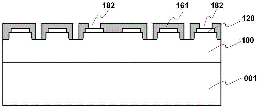
[0048] Please see attached image 3 The main difference between this embodiment and Embodiment 1 is that the areas of the P and N regions 130p and 130n of the electrode pad layer are close to or substantially the same. Specifically, it is achieved by the following method: an insulating layer 160 is provided on the P and N ohmic contact layers 122 and 121, and the N-type ohmic contact layer 121 is electrically insulated from the light-emitting layer and the p-type epitaxial layer of the LED epi...
Embodiment 3
[0050] In this embodiment, the lower surface of the end of the insulator 140 away from the light-emitting epitaxial stack protrudes from the lower surface of the electrode pad layer 130, which effectively prevents the short circuit between the P and N electrodes in the subsequent packaging process of the device. Assuming that the height difference between the relative position of the lower surface of the electrode pad layer 130 and the relative position of the lower surface of the insulator is H, and the gap D between the P and N regions of the electrode pad layer, this embodiment can be optimized by adjusting the size of H and D implementation effect. In this embodiment, the height difference H may be 20-100 μm, preferably 50 μm, and the gap D may be 20-100 μm, preferably 50 μm.
PUM
| Property | Measurement | Unit |
|---|---|---|
| thickness | aaaaa | aaaaa |
Abstract
Description
Claims
Application Information


