Semiconductor light-emitting device and manufacturing method thereof
A technology for light-emitting devices and manufacturing methods, which can be applied to semiconductor devices, electrical components, circuits, etc., and can solve the problems of poor heat dissipation capacity and low light extraction efficiency.
- Summary
- Abstract
- Description
- Claims
- Application Information
AI Technical Summary
Problems solved by technology
Method used
Image
Examples
Embodiment 1
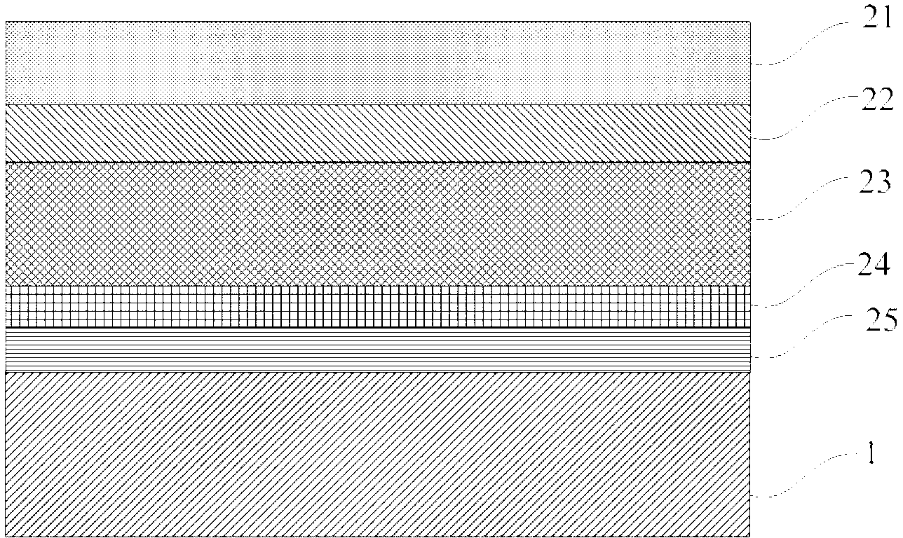
[0056] For the specific manufacturing method of the semiconductor light emitting device, please refer to the accompanying drawings.
[0057] see figure 1As shown, a semiconductor substrate is provided, preferably a 2-6 inch sapphire substrate 1 in this embodiment. An epitaxial layer (such as a GaN layer) is grown on the sapphire substrate 1 by metal-organic vapor deposition technology, and this layer includes a GaN buffer layer 25, an unintentionally doped gallium nitride layer 24, an N-type Ga layer 23 , light emitting region 22 and P-type GaN layer 21 .
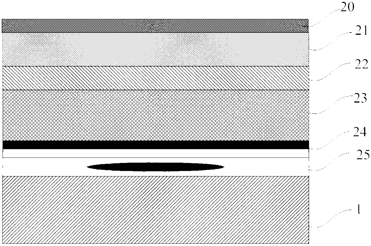
[0058] Then carry out the laser interface irradiation process, please refer to the attached figure 2 As shown, firstly, a protective layer 20 is deposited on the upper surface of the above-mentioned epitaxial layer (i.e., the surface) by plasma chemical vapor deposition technology. The material of the protective layer 20 can be silicon dioxide or silicon nitride, with a thickness of
[0059] Then adopt laser band or o...
example 2
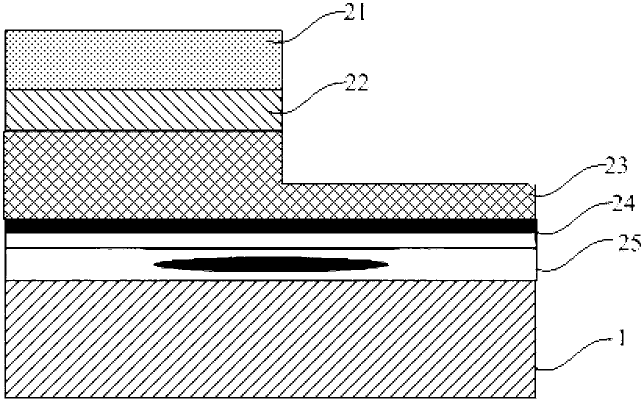
[0075] Example 2 is basically the same as Example 1, the difference is that the step of roughening the laser interface is obtained after obtaining image 3 The structure shown follows. That is, photolithography and etching techniques are used to perform partial etching to expose part of the N-type GaN layer 23 and then roughen the laser interface. The specific steps of the laser interface roughening process are as follows: First, a protective layer is deposited on the upper surface of the epitaxial layer (on the GaN surface) using plasma chemical vapor deposition technology. The material of the protective layer can be silicon dioxide or silicon nitride. , with a thickness of
[0076] Then adopt laser band or other shapes of continuous irradiation treatment, combined with the size of the chip, adjust the laser focus for interface irradiation. The focused interface is the GaN buffer layer. Because the crystal quality of the GaN buffer layer is poor, it is easier to absorb t...
PUM
 Abstract
Description
Claims
Application Information


