High-density type parallel transmission optical device
A high-intensity, light-transmitting technology, used in electromagnetic transceivers, coupling of optical waveguides, etc., can solve problems such as heat dissipation, affecting device performance, signal crosstalk, etc., to improve stability, reduce signal crosstalk, and reduce placement. The effect of precision requirements
- Summary
- Abstract
- Description
- Claims
- Application Information
AI Technical Summary
Problems solved by technology
Method used
Image
Examples
no. 1 example
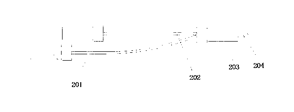
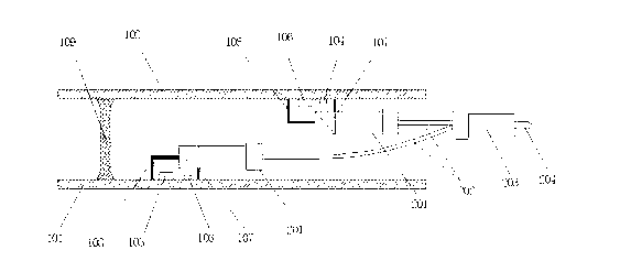
[0041] please see figure 1 , figure 2, the technical solution adopted in this first embodiment is: a high-intensity parallel transmission optical device, including: a transmitting PCB board 101, a receiving PCB board 102, a multi-channel transmitting chip 103, a multi-channel receiving chip 104, a transmitting drive Chip 105, receiving amplifier chip 106, multi-channel lens array 107, sealing cover 108, connecting line 109, transfer array fiber jumper assembly; multi-channel lens array 107 and sealing cover 108 are two; transfer array fiber The jumper assembly includes: multi-core standard MPO ferrule 201, ribbon fiber 202, standard MPO ferrule 203 with twice the number of cores and positioning guide post 204, two multi-core standard MPO ferrules 201, ribbon fiber 202 is two groups, and there are two positioning guide posts 204; the standard MPO ferrule 203 with twice the number of cores is respectively connected to two multi-core standard MPO ferrules 201 through two sets o...
no. 2 example
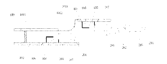
[0045] please see figure 1 , image 3 The only difference between the technical solution adopted in this second embodiment and the technical solution adopted in the first embodiment is that the transmitting PCB board 101 is composed of a first PCB hard board 1011, a first soft board 1012 and a second PCB hard board 1013, the first PCB hard board 1011 and the second PCB hard board 1013 are connected through the first soft board 1012. The multi-channel emission chip 103 and the emission driver chip 105 are mounted on the second hard PCB 1013 , and the multi-channel emission chip 103 and the emission driver chip 105 are electrically connected by gold wires.
[0046] The rest of the structure is exactly the same as that of the first embodiment, which can make the device space more favorable for layout.
no. 3 example
[0048] please see figure 1 , Figure 4 The only difference between the technical solution adopted in the third embodiment and the technical solution adopted in the first embodiment is that the receiving PCB board 102 is composed of a third PCB hard board 1021, a second soft board 1022 and a fourth PCB hard board 1023, the third PCB hard board 1021 and the fourth PCB hard board 1023 are connected through the second soft board 1022; the multi-channel receiving chip 104 and the receiving amplifier chip 106 are mounted on the fourth PCB hard board 1023, and the multi-channel receiving chip 104 It is electrically connected with the receiving amplifier chip 106 through a gold wire.
[0049] The rest of the structure is exactly the same as that of the first embodiment, which can make the device space more favorable for layout.
PUM
 Abstract
Description
Claims
Application Information


