A high-density parallel transmission optical device

A high-intensity, light-transmitting technology, applied in the field of CXP active optical cables and plug-in optical devices, can solve problems affecting device performance, signal crosstalk, heat dissipation, etc., to reduce signal crosstalk, reduce placement accuracy requirements, The effect of improving stability

Active Publication Date: 2015-08-12
WUHAN TELECOMM DEVICES
View PDF5 Cites 0 Cited by
  • Summary
  • Abstract
  • Description
  • Claims
  • Application Information

AI Technical Summary

Problems solved by technology

[0004] At the same time, the above-mentioned structure also has a certain problem of signal crosstalk, because the four chips: the multi-channel transmitting chip, the multi-channel receiving chip, the transmitting driver chip and the receiving amplifier chip are all installed on the same soft board. The wiring of the signal lines is concentrated, and the signal crosstalk between the transmitted signal and the received signal has a great influence, which will affect the performance of the device
[0005] Moreover, the above-mentioned structure still has a certain heat dissipation problem. Since the four chips: the multi-channel transmitter chip, the multi-channel receiver chip, the transmitter driver chip and the receiver amplifier chip are all installed on the same soft board, the heat dissipation problem is also a design bottleneck. one

Method used


Image

  • A high-density parallel transmission optical device
  • A high-density parallel transmission optical device
  • A high-density parallel transmission optical device

Examples


no. 1 example

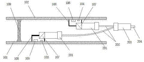
[0041] please see figure 1 , figure 2, the technical solution adopted in the first embodiment is: a high-intensity parallel transmission optical device, including: a transmitting PCB board 101, a receiving PCB board 102, and a multi-channel transmitting chip

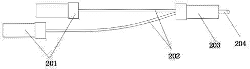
[0042] 103, multi-channel receiving chip 104, transmitting drive chip 105, receiving amplifier chip 106, multi-channel lens array 107, sealing cover 108, connecting line 109, transfer array fiber jumper assembly; multi-channel lens array 107 and sealing cover 108 are two; the transfer array fiber jumper assembly includes: multi-core standard MPO ferrule 201, ribbon fiber 202, standard MPO ferrule 203 with twice the number of cores and positioning guide post 204, multi-core standard MPO There are two ferrules 201, two sets of ribbon optical fibers 202, and two positioning guide posts 204; the standard MPO ferrule 203 with twice the number of cores passes through two sets of ribbon optical fibers 202 and two multi-core s...

no. 2 example

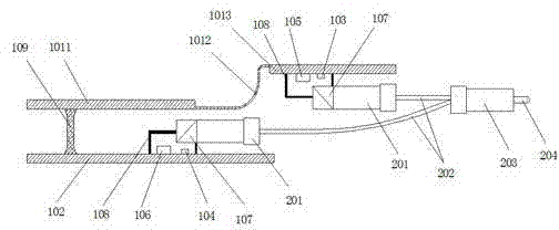
[0046] please see figure 1 , image 3 The only difference between the technical solution adopted in this second embodiment and the technical solution adopted in the first embodiment is that the transmitting PCB board 101 is composed of a first PCB hard board 1011, a first soft board 1012 and a second PCB hard board 1013, the first PCB hard board 1011 and the second PCB hard board 1013 are connected through the first soft board 1012. The multi-channel emission chip 103 and the emission driver chip 105 are mounted on the second hard PCB 1013 , and the multi-channel emission chip 103 and the emission driver chip 105 are electrically connected by gold wires.

[0047] The rest of the structure is exactly the same as that of the first embodiment, which can make the device space more favorable for layout.

no. 3 example

[0049] please see figure 1 , Figure 4 The only difference between the technical solution adopted in the third embodiment and the technical solution adopted in the first embodiment is that the receiving PCB board 102 is composed of a third PCB hard board 1021, a second soft board 1022 and a fourth PCB hard board 1023, the third PCB hard board 1021 and the fourth PCB hard board 1023 are connected through the second soft board 1022; the multi-channel receiving chip 104 and the receiving amplifier chip 106 are mounted on the fourth PCB hard board 1023, and the multi-channel receiving chip 104 It is electrically connected with the receiving amplifier chip 106 through a gold wire.

[0050] The rest of the structure is exactly the same as that of the first embodiment, which can make the device space more favorable for layout.


PUM


Abstract

The invention discloses a high-density type parallel transmission optical device which is applicable to a CXP encapsulating and plug type optical device and a CXP active optical cable (AOC), wherein the CXP encapsulating and plug type optical device and the CXP AOC are applied to data communication currently. The high-density type parallel transmission optical device comprises a transmitting PCB, a receiving PCB, a multi-path transmitting chip, a multi-path receiving chip, a transmission driving chip, a receiving amplifying chip, multi-path lens arrays, sealing cover plates and a connecting line, wherein the number of the multi-path lens arrays is two, and the number of the sealing cover plates is two. The high-density type parallel transmission optical device is characterized in that the parallel transmission optical device further comprises a changeover array optical fiber jumper assembly. The high-density type parallel transmission optical device is capable of effectively reducing the surface-mounting accuracy requirements of the multi-path transmitting chip and the multi-path receiving chip to further reduce encapsulating difficulty, effectively solving the signal crosstalk problem and the radiating problem, and improving the performance stability.

Description

technical field [0001] The invention relates to a high-intensity parallel transmission optical device, which is applicable to the plug-in optical device in the CXP packaging form and the CXP active optical cable (AOC) in the current data communication application. Specifically, it relates to a parallel transmission optical device suitable for CXP packaging. Background technique [0002] At present, the main structure of the 12*10G CXP parallel transmission optical module in data communication applications is as follows. It consists of two PCB boards, the bottom board is the transmitting board, the top board is the receiving board, and the two boards are connected by a soft board. Mount a metal heat sink under the flexible board, and mount multiple transmitting chips, multiple receiving chips, transmitting driver chips and receiving amplifier chips on the relative positions above the flexible board in sequence, and use gold wire bonding to these The chip is connected with a ...

Claims


Application Information

Patent Timeline
Patent Type & Authority Patents(China)
IPC IPC(8): G02B6/42G02B6/43H04B10/40
Inventor 曹芳张德玲杨昌霖何明阳王雨飞
Owner WUHAN TELECOMM DEVICES
Why Eureka
Try Eureka