
Step-type micro convex point structure and preparation method thereof

A micro-bump and step-type technology, which is applied in semiconductor/solid-state device manufacturing, electrical components, electric solid-state devices, etc., can solve problems such as short circuit between micro-bumps, larger diameter of micro-bumps, and easy collapse, so as to ensure The effect of processing control accuracy, reducing PCB size, and simple and compact structure

Inactive Publication Date: 2013-09-25
NAT CENT FOR ADVANCED PACKAGING
View PDF3 Cites 3 Cited by
  • Summary
  • Abstract
  • Description
  • Claims
  • Application Information

AI Technical Summary

Problems solved by technology

In the existing flip-chip packaging and wafer-level packaging, the distance between the micro-bump structures is relatively small, and the solder cap of the micro-bump structure with a small distance is easy to collapse during reflow, thereby causing a short circuit between the micro-bumps
[0003] In addition, flip-chip has certain requirements for the height of the micro-bump structure. When the height of the micro-bump structure is high, due to the poor control precision of the thick glue process, the diameter of the micro-bump will also become larger, which will affect the flip chip. The development of micro-bumps in the direction of high density will also correspondingly increase the difficulty and cost of PCB (Printed Circuit Board) board manufacturing process and the development of miniaturization

Method used


Image

  • Step-type micro convex point structure and preparation method thereof
  • Step-type micro convex point structure and preparation method thereof
  • Step-type micro convex point structure and preparation method thereof

Examples


Embodiment Construction

[0031] The present invention will be further described below in conjunction with specific drawings and embodiments.

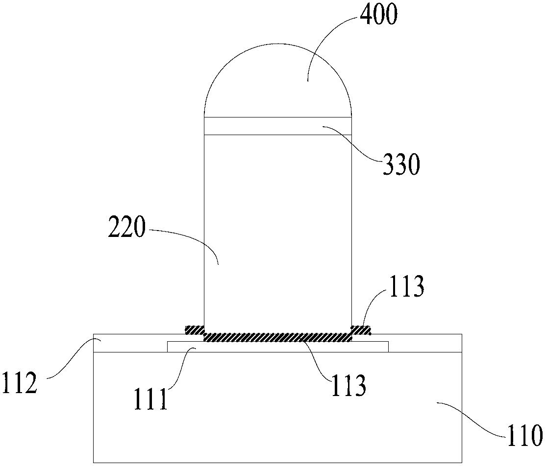
[0032] Such as figure 1 Shown: is the structure diagram of the existing micro-bump structure, the micro-bump structure includes a substrate body 110, a connection electrode layer 111 is arranged on one surface of the substrate body 110, and the connection electrode layer 111 covers the substrate body 110, and is electrically connected to the substrate body 110, the other side surface where the connection electrode layer 111 is connected to the substrate body 110 is covered with a passivation layer 112, and the connection electrode layer 111 and the substrate body 110 are protected by the passivation layer 112, The passivation layer 112 is etched to form an UBM layer 113 , and the UBM layer 113 passes through the passivation layer 112 and is electrically connected to the connecting electrode layer 111 . The UBM layer 113 is provided with a metal post 220, the l...


PUM


Abstract

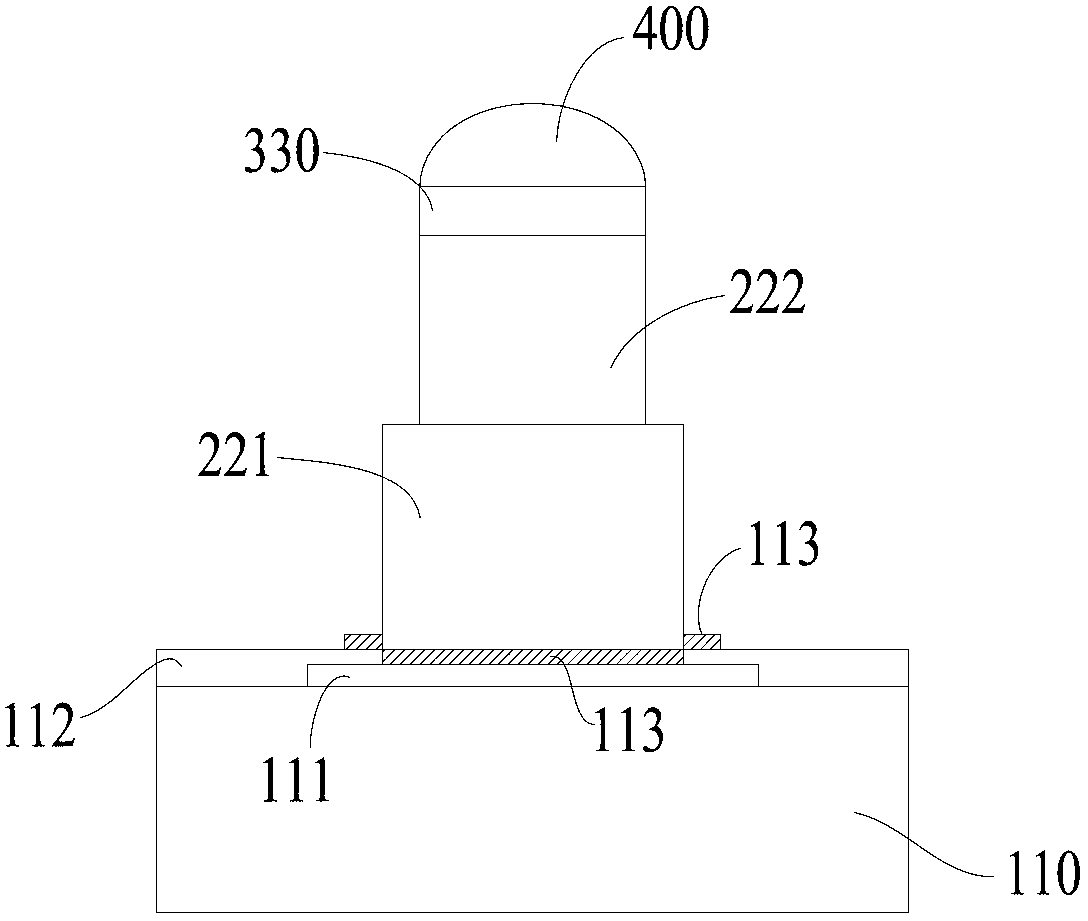
The invention relates to a micro convex point structure and a preparation method of the micro convex point structure, in particular to a step-type micro convex point structure and a preparation method of the step-type micro convex point structure, and belongs to the technical field of semiconductor packaging. According to the technical scheme, the step-type micro convex point structure comprises a substrate body, a connecting electrode layer, a passivating layer and a convex point lower metallizing layer, wherein the connecting electrode layer, the passivating layer and the convex point lower metallizing layer are located on the substrate body, and a metal pillar is arranged on the convex point lower metallizing layer. The metal pillar at least comprises a first pillar body layer and a second pillar body layer located on the first pillar body layer, wherein the first pillar body layer is in electric connection with the convex point lower metallizing layer, a step is formed between the second pillar body layer and the first pillar body layer, a blocking metal layer is arranged on the second pillar body layer, and a soldering flux cap is arranged on the blocking metal layer. The step-type micro convex point structure and the preparation method of the step-type micro convex point structure are simple and compact in structure, simple in manufacturing process and high in control accuracy, avoids a short circuit accident of a packaging structure, and improves reliability of packaging.

Description

technical field [0001] The invention relates to a micro-bump structure and a preparation method thereof, in particular to a stepped micro-bump structure and a preparation method thereof, belonging to the technical field of semiconductor packaging. Background technique [0002] The microbump structure can be used in flip-chip packaging as well as semiconductor packaging in wafer-level packaging. In the existing flip-chip packaging and wafer-level packaging, the distance between the micro-bump structures is relatively small, and the solder caps of the micro-bump structures with smaller distances tend to collapse during reflow, thereby causing short circuits between the micro-bumps. [0003] In addition, the flip chip has certain requirements for the height of the micro-bump structure. When the height of the micro-bump structure is high, the diameter of the micro-bump will also become larger due to the poor control accuracy of the thick glue process, which will affect the flip ...

Claims


Application Information

Patent Timeline
Patent Type & Authority Applications(China)
IPC IPC(8): H01L23/485H01L21/60
CPCH01L24/11H01L2224/11H01L2224/13H01L2224/13083H01L2924/00012
Inventor 王宏杰陆原
Owner NAT CENT FOR ADVANCED PACKAGING
Learn More