Method for manufacturing nitride gradient energy gap resonance tunneling ohmic contact

A technology of ohmic contact and resonant tunneling, which is applied in semiconductor/solid-state device manufacturing, electrical components, circuits, etc., can solve the problems of increasing ohmic contact resistance and depleting two-dimensional electrons, so as to reduce contact resistance and increase tunneling Through the current, improve the effect of tunneling current

Active Publication Date: 2013-10-02
NO 55 INST CHINA ELECTRONIC SCI & TECHNOLOGYGROUP CO LTD
View PDF6 Cites 3 Cited by
  • Summary
  • Abstract
  • Description
  • Claims
  • Application Information

AI Technical Summary

Problems solved by technology

However, reducing the barrier height and thinning the barrier will deplete the two-dimensional electrons in the heterojunction channel well, and raise the well site and the barrier of the well edge of the channel well, preventing the tunneling of low-energy electrons in the metal to the

Method used


Image

  • Method for manufacturing nitride gradient energy gap resonance tunneling ohmic contact

Examples


Embodiment 1

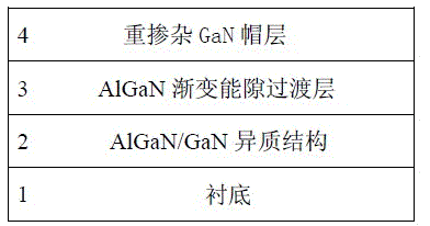
[0021] Consider the most commonly used by Al 0.3 Ga 0.7 Heterostructure 2 composed of N barrier layer and GaN channel layer. The simulation calculation shows that the electron gas density is 9.27*10 12 cm -2 . After covering the AlGaN gradient transition layer 3 and the heavily doped GaN cap layer 4 on the heterostructure, self-consistently solve the Schrödinger equation and Poisson equation, and optimize the design by doping concentration 3*10 19 cm -3 The 8nm GaN cap layer 4 and the Al composition ratio increase linearly from 0 to 0.3, and the doping concentration is 2*10 19 cm -3 and the graded-gap resonant tunneling ohmic contact formed by the graded-gap transition layer 3 with a thickness of 15 nm. The simulation calculation shows that the ground state energy level in the channel well is -0.84eV, and the quantum confinement energy level in the middle well is -0.79eV. The energy level difference is only 0.05eV, and the three-dimensional electrons on the metal elect...

Embodiment 2

[0023] In the research of millimeter-wave high-frequency devices, in order to improve the control of the gate electrode on the channel conductance and weaken the short-channel effect, a thin barrier with a high Al composition ratio must be used. Considered by 8nmAl 0.5 Ga 0.5 Heterostructure 2 composed of N barrier layer and GaN channel layer. The simulation calculation shows that the electron gas density is 1.298*10 13 cm -2 . After covering the AlGaN gradient transition layer 3 and the heavily doped GaN cap layer 4 on the heterostructure, self-consistently solve the Schrödinger equation and Poisson equation, and optimize the design by doping concentration 3*10 19 cm -3 The 8nm GaN cap layer 4 and the Al composition ratio increase linearly from 0 to 0.5, and the doping concentration is 2.2*10 19 cm -3The graded-gap resonant tunneling ohmic contact formed by the graded-gap transition layer 3 with a thickness of 20 nm. The simulation calculation shows that the ground st...

Embodiment 3

[0025] In order to strengthen the quantum confinement of the channel well and suppress the alloy scattering in the AlGaN alloy layer, many authors have studied the AlN / GaN superlattice barrier to replace the AlGaN alloy layer barrier. Consider a heterostructure 2 consisting of five sets of 1.8nmGaN / 0.8nmAlN heterojunction layers consisting of a superlattice barrier layer and a GaN channel layer. The simulation calculation shows that the electron gas density is 1.29*10 13 cm -2 . After covering the AlGaN gradient transition layer 3 and the heavily doped GaN cap layer 4 on the heterostructure, self-consistently solve the Schrödinger equation and Poisson equation, and optimize the design by doping concentration 3*10 19 cm -3 The ratio of the 8nm GaN cap layer 4 to Al increases linearly from 0 to 0.4, and the doping concentration is 2*10 19 cm -3 The graded-gap resonant tunneling ohmic contact formed by the graded-gap transition layer 3 with a thickness of 20 nm. The simulat...


PUM

PropertyMeasurementUnit
Thicknessaaaaaaaaaa

Abstract

The invention discloses a method for manufacturing nitride gradient energy gap resonance tunneling ohmic contact. According to the method, an AlGaN/GaN heterostructure 2, an AlGaN gradient energy gap depletion layer 3 and a heavy doping GaN cap layer 4 are sequentially grown on a substrate 1 so as to manufacture the ohmic contact; the heavy doping GaN cap layer 4 can reduce the contact barrier of a metal-semiconductor; the gradient energy gap depletion layer 3 forms a middle trap to reduce the resistance of the ohmic contact through the resonance tunneling. According to the invention, by the design of the middle trap of the a gradient energy gap, the metal-semiconductor contact barrier generated in the high-temperature alloy process is separated from the heterojunction barrier, and energy bands of double-barrier and single-trap heterostructures are optimally designed respectively, so that the tunneling current is obviously increased, and the ohmic contact is reduced. Meanwhile, with the design of the heavy doping GaN cap layer, the high-temperature alloy process is omitted; the surface appearance, the device performance and the reliability of the contact are improved.

Description

technical field [0001] The invention relates to a method for manufacturing a nitride semiconductor device, in particular to a method for making an ohmic contact on a nitride heterojunction. Specifically, the AlGaN gradient transition layer and the heavily doped GaN cap layer are grown on the nitride heterostructure by the energy band tailoring method to reduce the surface barrier height and thin the surface barrier, and increase the metal-semiconductor contact. barrier tunneling current. And using the energy band tailoring method, the thickness, energy band gradient and doping concentration of the AlGaN energy band transition layer are optimally designed, and an intermediate well is formed in the transition layer energy band. Cut the energy band of the intermediate well, so that the quantum confinement state in the intermediate well and the two-dimensional electronic state in the heterojunction channel well produce resonant tunneling, so that the electrons tunneling into the ...

Claims


Application Information

Patent Timeline
IPC IPC(8): H01L21/336
Inventor 薛舫时
Owner NO 55 INST CHINA ELECTRONIC SCI & TECHNOLOGYGROUP CO LTD
Why Eureka
Try Eureka