Image sensor and forming method thereof

An image sensor and device technology, applied in the field of image sensing, can solve problems such as high cost, difficult process control, complex image sensor forming process, etc., and achieve the effects of saving process steps, improving image sensing ability, and increasing the amount of light

Active Publication Date: 2013-10-02
SHANGHAI HUAHONG GRACE SEMICON MFG CORP
View PDF6 Cites 13 Cited by
  • Summary
  • Abstract
  • Description
  • Claims
  • Application Information

AI Technical Summary

Problems solved by technology

[0008] However, the formation process of the above-mentioned image sensor is relatively complicated, the process is not easy to control, and the cost is high

Method used


Image

  • Image sensor and forming method thereof
  • Image sensor and forming method thereof
  • Image sensor and forming method thereof

Examples


no. 1 example

[0043] The first embodiment of the present invention provides a method for forming an image sensor, please refer to Figure 5 to Figure 9 , is a schematic cross-sectional structure diagram of the formation process of the image sensor according to the first embodiment of the present invention.

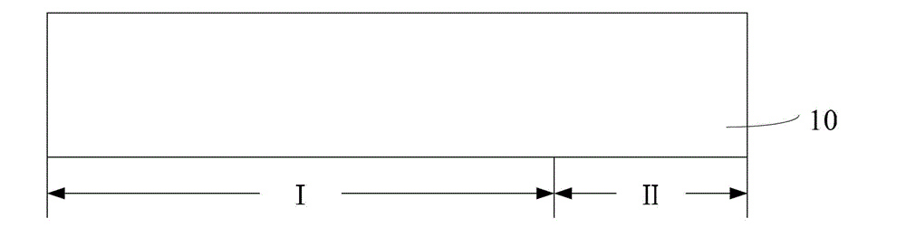
[0044] Specifically, please refer to Figure 5 , providing a semiconductor substrate 100, and the semiconductor substrate 100 includes a pixel array region I and a peripheral device region II.

[0045] The semiconductor substrate 100 is a silicon substrate, a germanium substrate, a silicon carbide substrate, a silicon germanium substrate, a silicon-on-insulator substrate, or the like. The semiconductor substrate 100 is doped with P-type or N-type ions. In this embodiment, the semiconductor substrate 100 includes a heavily doped P-type silicon substrate 101 and a lightly doped P-type silicon epitaxial layer 102 located on the surface of the P-type silicon substrate 101 .

[0046] The ...

no. 2 example

[0075] The second embodiment of the present invention also provides a method for forming an image sensor, please refer to Figure 10 ~ Figure 15 , is a schematic cross-sectional structure diagram of the formation process of the image sensor according to the second embodiment of the present invention.

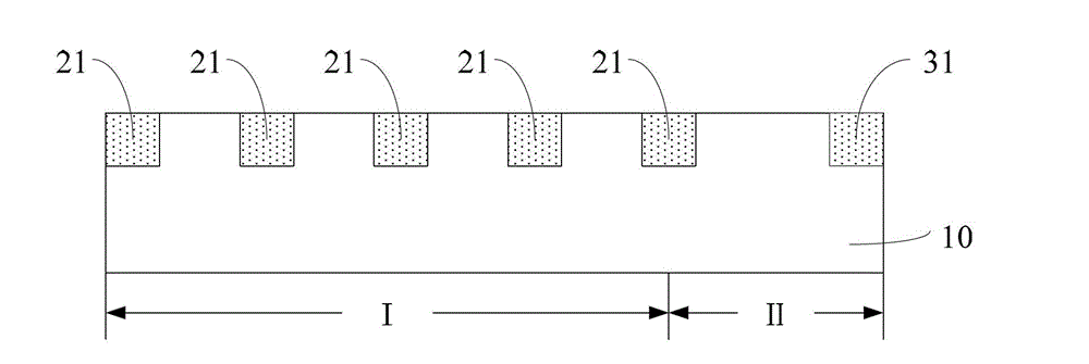
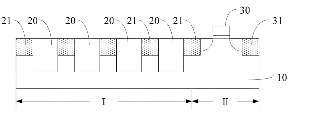
[0076] Specifically, please refer to Figure 10 , providing a semiconductor substrate 200, and the semiconductor substrate 200 includes a pixel array region I and a peripheral device region II. The semiconductor base 200 includes a heavily doped P-type silicon substrate 201 and a lightly doped P-type silicon epitaxial layer 202 on the surface of the P-type silicon substrate 201 .

[0077] Please refer to Figure 11 , forming a third mask layer 210 on the surface of the semiconductor substrate 200, and the third mask layer 210 exposes the surface of the semiconductor substrate 200 corresponding to the first shallow trench isolation structure and the second shallow trench isolat...


PUM


Abstract

The invention relates an image sensor and a forming method thereof. The image sensor comprises a semi-conductor substrate, a plurality of pixel units in a pixel array area and logic circuit devices in a peripheral device area, wherein the semi-conductor substrate comprises the pixel array area and the peripheral device area; every two adjacent pixel units are isolated from each other through a first shallow groove isolation structure; every two adjacent logic circuit devices are isolated from each other through a second shallow groove isolation structure; the first shallow groove isolation structures are deeper than the second shallow groove isolation structures. As the pixel units are isolated from one another only by the deeper first shallow groove isolation structures, and a P-type well region is not needed to be formed, processing steps are reduced; as the first shallow groove isolation structures are mainly used for isolating photoelectrons produced by photodiodes from crosstalk, and the working voltage corresponding to transistors in the pixel units is lower, and the first shallow groove isolation structures can effectively conduct electrical isolation even the first shallow groove isolation structures have bubbles.

Description

technical field [0001] The invention relates to the field of image sensing, in particular to an image sensor and a forming method thereof. Background technique [0002] Image sensors have been widely used in still digital cameras, mobile phone cameras, digital video cameras, medical camera devices (such as gastroscopes), automotive camera devices, etc., to sense the light projected on the semiconductor substrate and convert it into electrical signals accordingly. form an image signal. An image sensor generally includes a pixel array area composed of several pixel units and a peripheral device area electrically connected to the pixel units. The pixel array area includes photodiodes and other corresponding transistors (such as reset transistors, transfer transistors, etc.), the photodiodes are used to convert external light into photoelectrons, and other transistors connected to the photodiodes are used to convert photoelectrons into electrical signals. The peripheral device...

Claims


Application Information

Patent Timeline
Patent Type & Authority Applications(China)
IPC IPC(8): H01L27/146H01L27/148
Inventor 令海阳
Owner SHANGHAI HUAHONG GRACE SEMICON MFG CORP
Why Eureka
Try Eureka